L-shaped Resonant Microring Modulator
- Category: Nanotechnology, Optics & Photonics
- Tags: erman timurdogan, michael watts
On- and off-chip bandwidth and energy scaling are pushing the limits of CMOS and VCSEL technology, which allow only a single channel per fiber or wire. Wavelength-division multiplexed (WDM) systems based on silicon photonic interconnects can enable high-bandwidth, energy-efficient communications. Integrated resonant modulators play a major role in such links. Resonant silicon modulators utilize the plasma dispersion effect through free-carrier injection or depletion of a diode. Compact 3.5-μm microdisk modulators have been demonstrated with a power consumption of only 3 fJ/bit at 1-Vpp and 12.5 Gb/s operation[1]. Recently, 25Gb/s operation with 13fJ/bit at 1.2Vpp has been demonstrated with ~6-μm diameter microdisk modulator[2]. However, the microdisk inherently supports spurious modes that corrupt the free spectral range (FSR) by introducing unwanted resonance dips on the transmission. Therefore, only half of the FSR can be used for WDM channels in a silicon photonic link. Microrings eliminate the undesired modes, but directly contacting the microring induces scattering loss. External ridge based modulators increase the diameter to ~5-10 μm due to low confinement, thereby increasing the area and power. Recently, a 4-μm diameter adiabatic resonant microring modulator, which enabled single-mode operation by adiabatic tapering of the single mode waveguide, was demonstrated but limited to 12.5 Gb/s operation due to electrical resistance of the contacts[3].
In our paper[4], we introduce a new class of modulators, L-shaped resonant microrings (LRM) (Figure 1a), which allow for both hard outer walls and single mode propagation while maintaining low resistance electrical contacts. Thus, LRM modulators can have a compact size, high quality factor, and an uncorrupted FSR (Figure 1b) while maintaining high-speed operation. To allow for interior contacts, a hybrid junction consisting of a vertical and interdigitated p-n junction (Figure 1a) is formed. Frequency shifts and spectral response are shown in Figure 1c. Here, we demonstrate the LRM modulator operating in depletion mode, with data rates up to 30 Gb/s (Figure 1d), occupying chip area of < 20 µm2 and maintaining an uncorrupted 5.3 THz FSR (Figure 1b).
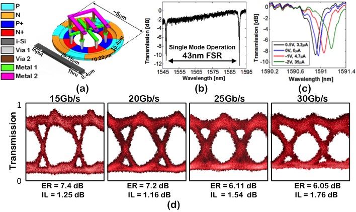
Figure 1: a) 3D sketch of the LRM modulator showing size, doping, and metal connections. b) Spur-free single mode operation of the LRM modulator with an FSR of 5.3 THz. c) Spectral response of the LRM modulator with respect to voltage dropped and current passing through the device. d) High speed measured optical eye diagrams at 15-, 20-, 25-, and 30-Gb/s data rates of the LRM modulator, driven by a PRBS data of 2.2Vpp with a -0.6V DC bias. Dynamic insertion loss and extinction ratio are denoted below the eye diagrams.
- M. R. Watts, W. A. Zortman, D. C. Trotter, R. W. Young, and A. L. Lentine, “Vertical junction silicon microdisk modulators and switches,” Opt. Exp., vol. 19, no. 22, pp. 21989–22003 2011. [↩]
- E. Timurdogan, C. M. Sorace-Agaskar, A. Biberman, and M. R. Watts, “Vertical Junction Silicon Microdisk Modulators at 25Gb/s,” in Proc. OFC/NFOEC, paper OTh3H.2 2013. [↩]
- A. Biberman, E. Timurdogan, W. Zortman, D. Trotter, and M. R. Watts, “Adiabatic microring modulators,” Opt. Exp., vol. 20, no. 28, pp. 29223-29236 2012. [↩]
- E. Timurdogan, C. M. Sorace-Agaskar, and M. R. Watts, “L-Shaped Resonant Microring (LRM) Modulator,” in Proc. OIC, paper MC2 2013. [↩]