Vertical Junction Silicon Microdisk Modulators at 25Gb/s
- Category: Nanotechnology, Optics & Photonics
- Tags: erman timurdogan, michael watts
High-performance computing systems require high bandwidth, low power, and scalable optical interconnects to maintain balanced communications in future exascale machines. Low-power, low-voltage, high-speed, and compact CMOS-compatible silicon electro-optic modulators are key enablers for next generation optical interconnects. Silicon modulators based on the free-carrier effect in silicon achieve high-speed modulation by injecting or depleting charge, inducing a frequency shift in a Mach-Zehnder interferometer or resonant device that translates the resultant frequency shift into an amplitude response. Resonant modulators confine light in compact high-Q devices, enhancing the interaction of the light with the change in charge distribution. Compact resonant devices also minimize the device capacitance, enabling high-speed and low power modulators. In previous record-setting demonstrations, vertical p-n junction devices have achieved error-free modulation up to 12.5Gb/s with only a 1V drive and while consuming only 3fJ/bit[1].
In our work[2], we experimentally demonstrate the first vertical junction silicon microdisk modulator (Figure 1a-b) to achieve open eye-diagrams at a data rate of 25Gb/s (Figure 1d) and error-free operation up to 20Gb/s. A circular overlapping p+ and n+ doping profile within circularly contacted microdisk modulators (Figure 1a-b) reduce the device resistance and enable high-speed operation while maintaining a hard outer wall for maximizing the optical confinement. Frequency shifts and spectral response is shown in Figure 1c. The device represents the smallest silicon modulator to run at 25Gb/s and achieves the lowest reported power penalty compared to a commercial LiNbO3 modulator [2], important for the overall power budget in a microphotonic link.
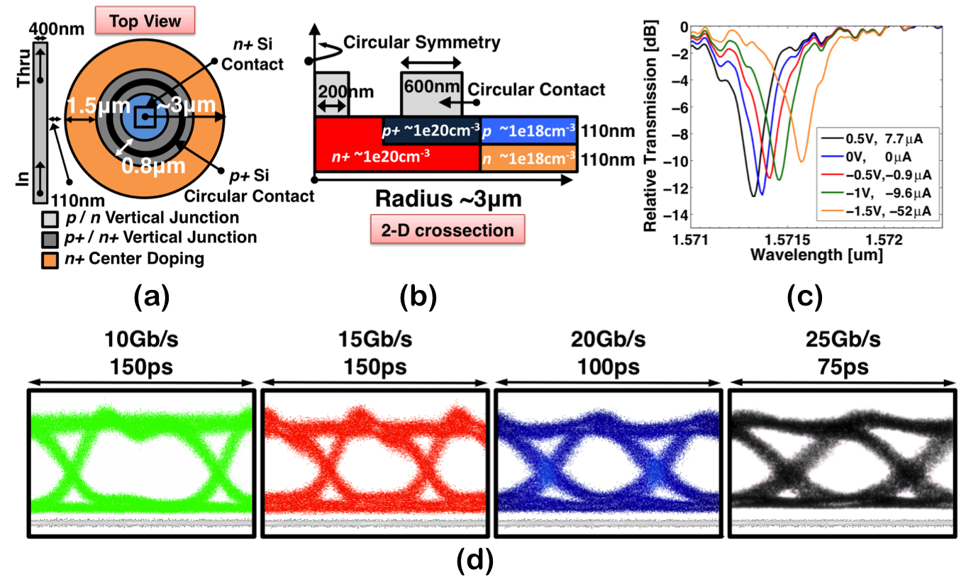
Figure 1: a) Top-view of the 6-µm-diameter microdisk modulator, which utilizes circular inner contacts. b) 2D cross-section showing the doping profile with p-n vertical junction, p+and n+ overlapping regions. c) Spectral response of the microdisk modulator with respect to voltage dropped and current passing through the microdisk modulator. d) High-speed measured optical eye diagrams at 10-, 15-, 20-, and 25-Gb/s data rates of the microdisk modulator, driven by AC coupled 1.2Vpp. The eye diagrams are shown with the true zero (gray line) at each data rate.
- M. R. Watts, W. A. Zortman, D. C. Trotter, R. W. Young, and A. L. Lentine, “Vertical junction silicon microdisk modulators and switches,” Opt. Exp., vol. 19, no. 22, pp. 21989–22003 2011. [↩]
- E. Timurdogan, C. M. Sorace-Agaskar, A. Biberman, and M. R. Watts, “Vertical Junction Silicon Microdisk Modulators at 25Gb/s,” in Proc. OFC/NFOEC, paper OTh3H.2 2013. [↩]