- Leadership: Professor Tomas Palacios, Director
The MIT/MTL Center for Graphene Devices and Systems (MIT-CG) brings together, MIT researchers and industrial partners to advance the science and engineering of graphene-based technologies.
The center explores advanced technologies and strategies that enable graphene-based materials, devices and systems to provide discriminating or break-through capabilities for a variety of system applications ranging from energy generation and smart fabrics and materials, to RF communications and sensing. The MIT-CG supports the development of the science, technology, tools and analysis for the creation of a vision for the future of graphene-enabled systems.
Membership privileges for MIT-CG include:
Stay abreast of research developments in graphene
• Webcast of seminars
• Complimentary attendance to meetings
• Facilitated access to IP
Interact with students and faculty at MIT-GC events
• Industry Focus Day
• Resume book of graduating students
Participate in working groups of leading companies and researchers in defining the path forward for graphene
• Timely white papers on key issues
Collaborate with leading researchers on research that addresses today’s challenges
• Direct student projects on modeling in support of working group activities
• Pre-competitive teaming
- Authors: M. S. Dresselhaus, P. T. Araujo
- Sponsorship: NSF
Paulo T. Araujo has been using MTL facilities through 2011/2012 to fulfill one step of his device fabrication. In general, the devices are made by graphite exfoliation so that a single layer of graphene is sitting on a 300-nm-thick layer of SiO2. After the standard lithography steps used to design from two to four contacts over the graphene layer, titanium and gold are deposited. The metals are deposited by utilizing the e-beam evaporator from EML at MTL headquarters. The devices were used in gate-modulated Raman experiments, which allow us to observe phonon energy renormalizations by observing gate-voltage dependent changes in its Raman signatures [] [] [] [] .
- Authors: H. Park, P. R. Brown, V. Bulović, J. Kong
- Sponsorship: Eni S.p.A, Fannie and John Hertz Foundation, NSF
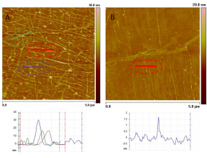
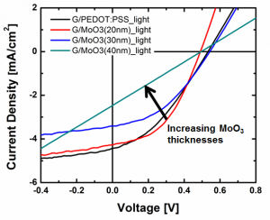
Due to the remarkable physical properties of graphene, applications in various areas such as transistors [] , chemical sensors [] , and logic devices [] have been explored; a variety of proof-of-concept devices have been demonstrated. In this work, organic photovoltaics (OPV) with graphene electrodes are constructed so that the effects of graphene morphology (Figure 1), hole transporting layers (HTL) (Figure 2), and counter electrodes are presented. One of the challenges in the integration of graphene in OPV is the incompatibility between the graphene electrode and poly(3,4-ethylenedioxythiophene):poly(styrenesulfonate) (PEDOT:PSS) hole transport layer (HTL) which significantly increases the device failure rate [] . When hydrophilic PEDOT:PSS is spin-coated onto graphene, it is difficult to achieve uniform and conformal coating due to the hydrophobic nature of the graphene surface, i.e., lower surface free energy. Instead of the conventional PEDOT:PSS HTL, an alternative transition metal oxide HTL (molybdenum oxide (MoO3)) is investigated to address the issue of surface immiscibility between graphene and PEDOT:PSS. The graphene films considered here are synthesized via low-pressure chemical vapor deposition (LPCVD) using a copper catalyst, and experimental issues concerning the transfer of synthesized graphene onto the substrates of OPV are discussed. The morphology of the graphene electrode and HTL wettability on the graphene surface are shown to play important roles in the successful integration of graphene films into the OPV devices. The effect of various cathodes on the device performance is also studied. These factors (i.e., suitable HTL, graphene surface morphology and residues, and the choice of well-matching counter electrodes) will provide better understanding for utilizing graphene films as transparent conducting electrodes in future solar cell applications.
-

-
Figure 1: AFM images of graphene morphology of different numbers of layers: (A) 3 layers and (B) 1 layer. Cross-sectional profiles of dotted regions are shown below. Much denser concentration of wrinkles on 3-layered graphene films are observed compared to a single-layer graphene sheet. The surface of stacked layers is thus much rougher than the single-layer sheet with a rms roughness more than 3-fold higher: 2.0 nm for 3 layers and 0.6 nm for 1 layer.
-

-
Figure 2: Current density vs. voltage characteristics of graphene OPV devices with PEDOT:PSS and MoO3 hole transporting layers with varying MoO3 HTL thicknesses (20-40 nm) under simulated AM 1.5G illumination at 100 mW/cm2. By utilizing the thermally evaporated MoO3 HTL, the wetting of HTL on graphene surface can be improved compared to the conventional PEDOT:PSS HTL.
- Authors: X. Zhang, K. K. Kim, J. Kong, M. Dresselhaus, T. Palacios
Graphene, a two-dimensional honeycomb lattice of sp2-hybridized carbon atoms, has attracted tremendous interest in the scientific community. Surface functionalization is a technology to engineer its electronic properties and make it even more desirable and controllable for electronic device applications. For example, chemical functionalization of graphene, especially by hydrogen, fluorine, and chlorine is predicted to enable doping, edge passivation, and opening of its bandgap. Here, we demonstrate that exposure of graphene device to chlorine plasma in an electron cyclotron resonance (ECR) plasma etcher is an effective way to tune the Fermi level of graphene carriers towards p-type direction, without sacrificing its high conductivity.
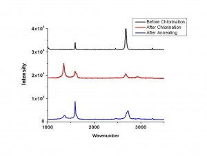
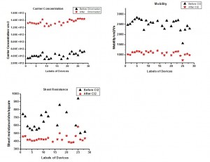
Figure 1 compares the Raman spectroscopy of graphene before and after chlorine plasma treatment and also shows how it changes after annealing. After chlorine plasma treatment for 30 s, the D band increases substantially while the G band blue shift by about 5 cm-1. More importantly, the D band decreases significantly after a 30-min annealing at 500 °C, which means little defect creation occurs during the plasma process. Further transport measurement shows that the carrier concentration in graphene increases considerably. The plasma reaction process tunes the Fermi level of an intrinsic p-type CVD graphene (VDirac >0) towards p-type direction further. We notice that the carrier mobility reduces after plasma reaction. However, this reduction should be mainly due to the increase of hole concentration in graphene rather than defect creation, which is confirmed by the decrease of its sheet resistance and increase of conductivity (see Figure 2). In addition, XPS analysis shows that the percentage of chlorine on the surface of graphene is around 20%. This approach indicates an important way to engineer graphene properties for high-performance applications of graphene devices.
-

-
Figure 1: Raman spectroscopy of graphene before plasma treatment, after plasma treatment, and after annealing.
-

-
FIgure 2: Comparison: conductivity, carrier concentration, mobility and sheet resistance of graphene devices before and after chlorination.
- Authors: B. Mailly-Giacchetti, F. Pappalardo, J. Kong, T. Palacios
- Sponsorship: STMicroelectronics, Institute for Soldier Nanotechnologies, International Iberian Nanotechnology Laboratory
With its all-surface 2D structure combined with very high carrier mobility, graphene is an extremely promising candidate for high sensitivity and low noise chemical sensing [] [] . Graphene devices can perform electrical detection for chemical sensing in many applications, e.g.,pH monitoring in electrolytes [] [] , measuring blood glucose, and in-vitro recording of the electrical activity of living cells [] . Integrating graphene on plastic substrates [] enables fabrication of low-cost, flexible sensors.
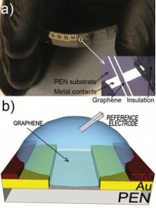
Our group has developed the first solution-gated graphene field effect transistor (SGFET) on a polyethylene naphthalate (PEN) substrate. These devices have important advantages with respect to traditional sensors, e.g., intrinsic signal amplification, simple electronic read-out, and straightforward integration with microelectronics. Fabrication of the SGFET starts with the transferring of graphene grown by chemical vapor deposition on the PEN substrate. Metal contacts were previously evaporated on the PEN substrate. Silicone rubber-based insulation was used to protect the metal contacts and wires from any contact with the electrolyte.
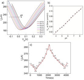
As Figure 2.a) shows, the characterization of our devices in a phosphate buffer solution demonstrates good transconductance, around 1 mS.mm-1, and carrier mobility of 300 cm2.V-1.s-1. Transconductance is 5 times smaller than that obtained for graphene on SiO2 which is due to the 10 times rougher surface of PEN compared to SiO2 and also the larger amount of PMMA residues remaining on graphene when transferred onto PEN. The pH measurements have been performed using these devices by recording how the Dirac point shifts with changes in pH, as Figure 2.b) shows. Sensitivity to 22 mV/pH has been demonstrated. In addition, long-term pH monitoring was shown for the first time in these graphene devices, as Figure 2.c) shows. Our on-going work focuses on functionalizing graphene to demonstrate new biosensors for glucose and E. coli detection on plastic substrate.
-

-
Figure 1: a) Optical image of graphene chemical sensor array on plastic substrate. Inset on bottom right corner shows detail . b) Schematic of a graphene-on-PEN solution-gated transistor.
-

-
Figure 2: Transfer characteristics of 50×1000-µm2 graphene-on-PEN SGFET at constant drain-source voltage of Vds=50 mV for different pHs. b) Dirac point shift with pH. c) Drain-source current vs. time data for pHs 9-4.
- Authors: L. Hsu, S. J. Ha, K. K. Kim, J. Kong, T. Palacios
- Sponsorship: ONR GATE-MURI, SRC/FCRP MSD, Institute of Soldier Nanotechnology

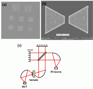
Figure 1: (a) Scanning electron microscopy (SEM) of bowtie array; (b) SEM of single element bowtie; (c) Fourier Transform infrared spectroscopy setup for characterization of graphene infrared photodetectors.
Graphene is a two-dimensional (2D) material that has attracted great interest for electronic devices since its discovery in 2004 [] . With essentially the same lattice structure as an unwrapped carbon nanotube, graphene shares many of its advantages, such as having the highest intrinsic carrier mobility at room temperature of any known material [] . This trait, combined with its high electron velocity and thermal conductivity, makes this carbon-based material an excellent candidate for high frequency electronic applications. Furthermore, graphene, due to its zero band gap band structure, also has a broadband optical absorption ranging from the far-infrared (λ>10 µm) all the way to the visible (λ< 532 nm) [] . Standard state-of-the-art infrared focal plane arrays rely on very exotic materials systems such as InSb and HgCdTe, both of which are difficult to grow as well as difficult to integrate cheaply with silicon read out electronics [] . Graphene, on the other hand, could enable a new generation of carbon-based infrared photodetectors.
Metal-graphene-metal photodetectors have been demonstrated in the visible range (532 nm) using exfoliated highly oriented pyrolytic graphite (HOPG); however, the external efficiencies of these devices are generally low (<1%) [] . Graphene photodetectors may intrinsically have efficiencies ranging from 10-15%; however, poor optical coupling with the incident light reduces the overall efficiencies of these devices. Therefore, to better address these issues, we have begun fabrication of large area photodetector arrays utilizing plasmonic antenna elements to better match the incoming light to the spatial response of the graphene photodetectors designed in the infrared (Figure 1 (a) and (b)). Furthermore, using chemically vapor grown graphene, we have been fabricating large array photodetector arrays (1 cm x 1 cm) to better extract power from the incident electromagnetic radiation. The setup for characterizing the optical properties of these photodetectors is shown in Figure 1(c).
- Authors: S. Ha, A. Hsu, T. Palacios, A. P. Chandrakasan
- Sponsorship: International Iberian Nanotechnology Laboratory, MIT/Army Institute for Soldier Nanotechnologies, Fulbright Science and Technology Award
The CMOS image sensor is widely used in digital multimedia applications. Its performance ramps up every year with denser integration, better noise suppression, adjustable dynamic range, and lower power [] . However, the band gap of silicon fundamentally limits the absorption spectrum to be in the visible and near-infrared light (λ < 1100nm) [] . In our research, we propose an integrated CMOS imager with a graphene photodetector. With the zero band gap, the graphene photodetector absorbs long-wavelengths (λ > 1μm) and enables integrated circuits for a wide spectrum of imaging applications such as thermal and terahertz imaging.
In the design of the graphene photodetector, graphene’s high conductivity is a key problem. When a bias voltage is applied to a graphene photodetector, the resulting leakage current easily dominates the photocurrent. Also, the low output impedance severely limits the output voltage of the graphene photodetector up to only a few microvolts, which degrades the signal-to-noise ratio (SNR). To resolve the leakage issue and improve SNR, we propose to use a modulated input source. The mechanical shutter working at around 1 kHz shifts the input signal out from the DC region where the leakage component dominates. The modulation also suppresses flicker noise in the photodetector and the readout circuits, by a band-pass filter followed by a multi-stage low-noise amplifier.
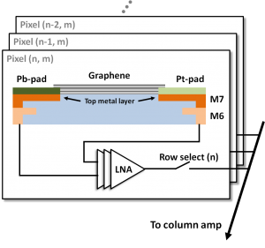
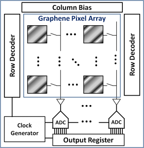
Figure 1 shows the pixel design of the photodetector. Unlike p-n junction photodiodes [] , the graphene photodetector is placed on top of the silicon substrate, requiring no extra area; as a result, higher integration can be achieved in each pixel. The amplitude of the photocurrent is measured by an 8b-resolution ADC in a column-parallel architecture as shown in Figure 2. By multiplexing each pixel, this architecture gives a good trade-off between frame rate and power consumption.
-

-
Figure 1: Image sensor pixel design with graphene photodetector and low-noise amplifiers.
-

-
Figure 2: Top view of the floor plan of wide spectrum image sensor IC.
