Graphene-based CMOS Infrared Imaging System
- Category: Circuits & Systems
- Tags: anantha chandrakasan, graphene, sungjae ha, tomas palacios
The CMOS image sensor is widely used in digital multimedia applications. Its performance ramps up every year with denser integration, better noise suppression, adjustable dynamic range, and lower power [1] . However, the band gap of silicon fundamentally limits the absorption spectrum to be in the visible and near-infrared light (λ < 1100nm) [2] . In our research, we propose an integrated CMOS imager with a graphene photodetector. With the zero band gap, the graphene photodetector absorbs long-wavelengths (λ > 1μm) and enables integrated circuits for a wide spectrum of imaging applications such as thermal and terahertz imaging.
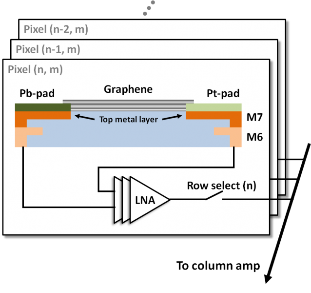
In the design of the graphene photodetector, graphene’s high conductivity is a key problem. When a bias voltage is applied to a graphene photodetector, the resulting leakage current easily dominates the photocurrent. Also, the low output impedance severely limits the output voltage of the graphene photodetector up to only a few microvolts, which degrades the signal-to-noise ratio (SNR). To resolve the leakage issue and improve SNR, we propose to use a modulated input source. The mechanical shutter working at around 1 kHz shifts the input signal out from the DC region where the leakage component dominates. The modulation also suppresses flicker noise in the photodetector and the readout circuits, by a band-pass filter followed by a multi-stage low-noise amplifier.
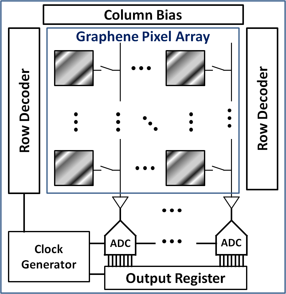
Figure 1 shows the pixel design of the photodetector. Unlike p-n junction photodiodes [3] , the graphene photodetector is placed on top of the silicon substrate, requiring no extra area; as a result, higher integration can be achieved in each pixel. The amplitude of the photocurrent is measured by an 8b-resolution ADC in a column-parallel architecture as shown in Figure 2. By multiplexing each pixel, this architecture gives a good trade-off between frame rate and power consumption.
-

- Figure 1: Image sensor pixel design with graphene photodetector and low-noise amplifiers.
-
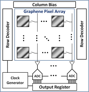
- Figure 2: Top view of the floor plan of wide spectrum image sensor IC.
- A. Fish and O. Yadid-Pecht, “Low power CMOS imager circuits,” in Circuits at the Nanoscale: Communications, Imaging, and Sensing, K. Iniewski, Ed. Boca Raton: CRC Press/Taylor & Francis, 2009. [↩]
- R. Kaufmann, “Near infrared image sensor with integrated germanium photodiodes,” Journal of Applied Physics, vol. 110, pp. 023107-6, July 2011. [↩]
- M. Perenzoni, N. Massari, D. Stoppa, L. Pancheri, M. Malfatti and L. Gonzo, “A 160×120-pixels range camera with in-pixel correlated double sampling and fixed-pattern noise correction,” IEEE Journal of Solid-State Circuits, vol. 46, pp. 1672-1681, July, 2011. [↩]