Towards a Self-aligned InGaAs Trigate MOSFET
- Category: Electronic Devices, Nanotechnology
- Tags: alon vardi, jesus del alamo
Si-based CMOS technology is approaching the limits of its capabilities, and as a result there is extensive research into looking for novel methods to further scale logic circuitry. III-V semiconductors are considered leading candidates for future deeply-scaled integrated technology[1]. The low-effective mass of various III-V materials such as InGaAs and InAs gives rise to extraordinarily high electron velocities, which promise transistors with high performance at low voltage.
The fundamental requirement for future switches is simple: maximum ON current (ION) for a given OFF current (IOFF) operating at a small voltage on a sub-10-nm scale. Unfortunately, there is a tradeoff between ION and IOFF as the dimensions scale down. There are two approaches to address this problem. First, the material properties can be adjusted by means of strain management or alternative channel material; second, the dimensionality can be modified to obtain better electrostatic control and higher current density for a given footprint. III-V Trigate-FETs employ both approaches and are expected to show an unprecedented ION/IOFF ratio at the 10-nm regime and under 0.5-V operation voltages.
This project aims to demonstrate the first self-aligned sub-10-nm InGaAs Trigate transistor. There are many challenges to overcome before III-V Trigates can be accepted as a valid alternative. Understanding how to etch high aspect ratio fins, curing etching damage, reducing the sidewalls’ interface state traps (Dit) and obtaining low access resistance are only few of the many difficulties that need to be faced. We are pursuing a device design and a process integration approach that will allow an aggressive scale-down of device dimensions. Figure 1 shows the fin- etch module test structure; we have fabricated InGaAs fins with sub-20-nm resolution using a novel RIE process. An aspect ratio as high as 10 and smooth sidewalls and surfaces have also been demonstrated (inset). Figure 2 shows the fin contacting scheme using Mo. To minimize the access resistance, the metal covers the source and drain top as well as the sidewalls.
Successful demonstration of self-aligned III-V Trigate is an important milestone of CMOS technology, which will allow Moore‘s law to be extended, safely, into the sub-10-nm regime, and we are closer than ever to making it happen.
-
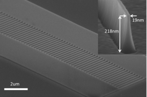
- Figure 1: Fin etch test structures: array of 100-nm fins (pitch 200 nm). Inset: demonstration of the fin geometry that we obtain in our process; the fin is 19-nm in width and 218-nm in height.
-

- Figure 2. SEM image of fin contact test structure. In this device, the Mo contact covers the top as well as the fin sidewalls. The bright lines in the fin cross-section separate the cap, channel, and buffer layers.
- J. A. del Alamo, “Nanometer-scale electronics with III-V compound semiconductors,” Nature, vol. 479, pp. 317-323, Nov. 2011. [↩]