Controlled Placement of Colloidal Quantum Dots in Sub-15-nm Clusters
Semiconductor colloidal quantum dots (QDs) are electronically quantized systems with promising applications in optoelectronic devices[1]. A key aspect of such systems is the fine control of optical properties in the synthesis process[2]. These QDs are predominantly used in thin-film arrangement, deposited by spin casting or dip coating. Single QD patterning is one of the major challenges to designing a system that takes advantage of individual properties of QDs[3]. Here we present a templated self-assembly technique to control the position of individual QDs through electron-beam lithography (EBL). This optimized top-down lithographic process is a step towards the integration of individual QDs in optoelectronics systems for industrial applications.
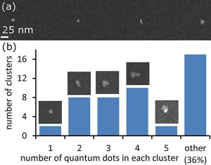
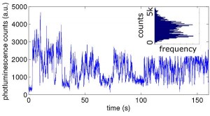
The fabrication process for QD placement occurred in four steps. First, a poly(methylmethacrylate) (PMMA) resist was spin coated on a silicon substrate to a thickness of 12 nm. Then, EBL was performed to obtain an array of holes (templates). The QD solution (6-nm-diameter CdSe or 5-nm-diameter CdSe/CdZnS) was spin cast or drop cast on top of the PMMA holes, and the remaining resist was removed by dissolution in acetone for 3 min[4]. This process resulted in QD clusters attached to the substrate, as shown in Figure 1. For the application of patterned QDs in excitonic or nano-optical devices, optical characterization is required. We investigated the resilience of the photoluminescence (PL) following the patterning process. The samples were observed with confocal scanning microscopy. Figure 2 shows PL signal of a sub-15-nm diameter QD cluster. Thus, the placed QD clusters may be used for further experiments and applications.
- Figure 1: (a) Scanning-electron micrograph of lithographically placed 6-nm-diameter CdSe QDs. The QD clusters were fabricated using PMMA holes with 8-15 nm diameter. (b) Histogram of the number of QDs in each cluster versus the number of clusters, for the sample in (a). We analyzed 54 sites designed for QD clusters. The QDs were counted from the SEM micrographs. Representative SEM images were added to the histogram.
- Figure 2: Photoluminescence time trace of a sub-15-nm diameter CdSe/CdZnS QD cluster that was placed by this method. The time trace shows intermittent luminescence (blinking). The inset shows PL intensity versus frequency. The PL intensity presented a bi modal distribution, indicating a blinking state of the placed QD cluster.
- A. P. Alivisatos, “Semiconductor Clusters, Nanocrystals, and Quantum Dots,” Science, vol. 271, no. 5251, pp. 933-937, (1996). [↩]
- S. A. Empedocles, D. J. Norris, and M. G. Bawendi, “Photoluminescence Spectroscopy of Single CdSe Nanocrystallite Quantum Dots,” Phys. Rev. Lett. vol. 77, pp. 3873-3876, (1996). [↩]
- J. Liddle, Y. Cui, and P. A. Alivisatos, “Lithographically directed self-assembly of nanostructures,” Journal of Vacuum Science & Technology B, vol. 22, pp. 3409-3414 (2004). [↩]
- V. R. Manfrinato, D. D. Wanger, D. B. Strasfeld, H. Han, F. Marsili, J. P. Arrieta, T. S. Mentzel, M. G. Bawendi, and K. K. Berggren, “Controlled placement of colloidal quantum dots in sub-15-nm clusters,” Nanotechnology, vol. 24, 125302 (2013). [↩]


