Resolution Limits of Electron-beam Lithography toward the Atomic Scale
- Category: Nanotechnology
- Tags: karl berggren, vitor manfrinato
Electron-beam lithography (EBL) readily enables the fabrication of sub-10-nm features[1]. However, the resolution limits of this technique at length scales smaller than 10 nm are not well understood. The known resolution-limiting factors of EBL are electron scattering, spot size, development process, and resist structure. We minimized the influence of electron scattering in our process by using 200-kV accelerated electrons. To minimize the spot size, we chose an aberration-corrected scanning transmission electron microscope (STEM) with 0.14-nm spot size as the exposure tool. STEM exposures at 200 keV have been done in conventional resists before[2],[3], resulting in feature sizes of 6 nm and resolution (i.e., pattern half period) of 15-nm half-pitch. However, the resolution-limiting factors were not systematically explored. In this work we did STEM exposures in hydrogen silsesquioxane (HSQ) at 200 keV. We then developed the structures with salty development ((J.. K. W. Yang and K. K. Berggren, “Using high-contrast salty development of hydrogen silsesquioxane for sub-10-nm half-pitch lithography,” Journal of Vacuum Science & Technology B, vol. 25, no. 6, pp. 2025-2029, Dec. 2007.)) and performed bright-field TEM metrology[4].
Figure 1 shows maximum resolution of 5-nm half-pitch and 2-nm feature size. The reduced spot size in the STEM was responsible for the minimum feature size achieved. To compare the resolution limit of this technique with others, we measured the point-spread function (PSF) by using single-pixel exposures and measuring the feature radii as a function of dosage. The radii from zero to 2 nm were not achieved experimentally. Thus from the structural shape shown in Figure 1D, we back-calculated the 200 keV PSF from zero to 20 nm radii, which we called “calculated PSF”[5]. We used the PSFs (measured and calculated) to calculate the energy-density contrast for a given pitch, as shown in Figure 2. The confined deposition of energy density at 200 keV translates into higher energy-density contrast, which was critical for achieving a higher resolution at 200 than at 30 keV.
-
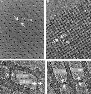
- Figure 1: TEM micrographs of 10-nm-thick HSQ on 10-nm-thick SiNx membrane substrate, exposed at 200 keV. (A) 10-nm-half-pitch HSQ dot array with 5.1± 0.8 nm feature size. (B) 5-nm-half-pitch HSQ dot array with 5.6 ± 1.2 nm feature size. The dose was (A) 18 and (B) 6 fC/dot. (C) and (D) are typical ~2 nm feature size with 8 nC/cm linear dose.
-
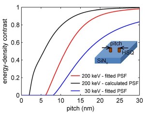
- Figure 2: Calculated energy-density contrast, K(p)=(Emax-Emin)/(Emax+Emin), for the fabrication of two adjacent posts at 30 and 200 keV exposures. The blue and red curves were calculated using the fitted PSF for 30 and 200 keV, respectively. The black curve is based on the calculated PSF, predicting higher resolution than using the fitted PSF at 200 keV.
- J.. K. W. Yang and K. K. Berggren, “Using high-contrast salty development of hydrogen silsesquioxane for sub-10-nm half-pitch lithography,” Journal of Vacuum Science & Technology B, vol. 25, no. 6, pp. 2025-2029, Dec. 2007. [↩]
- C. Vieu, F. Carcenac, A. Pépin, Y. Chen, M. Mejias, A. Lebib, L. Manin-Ferlazzo, L. Couraud, and H. Launois, “Electron beam lithography: Resolution limits and applications,” Applied Surface Science, vol. 164, pp. 111-117, Aug. 2000. [↩]
- S. Yasin, D. G. Hasko, and F. Carecenac, “Nanolithography using ultrasonically assisted development of calixarene negative electron beam resist,” Journal of Vacuum Science & Technology B, vol. 19, no. 1, pp. 311-313, Jan. 2001. [↩]
- H. Duan, V. R. Manfrinato, J. K. W. Yang, D. Winston, B. M. Cord, and K. K. Berggren, “Metrology for electron-beam lithography and resist contrast at the sub-10-nm scale,” Journal of Vacuum Science & Technology B, vol. 28, no. 6, pp. C6H11-C6H17, Dec. 2010. [↩]
- V. R. Manfrinato, L. Zhang, D. Su, H. Duan, R. G. Hobbs, E. A. Stach, and K. K. Berggren, “Resolution limits of electron-beam lithography toward the atomic scale,” Nano Letters, vol. 13, pp. 1555–155, 2013. [↩]