- Authors: C.-H. Hsieh, H. Xu, Y. Lu, H. Gao, B. Zhang, H. Sun, G. Barbastathis.
- Sponsorship: Singapore-MIT Alliance for Research and Technology – Independent Research Group: Center for Environmental Sensing and Modeling, Air Force Office of Scientific Research MURI, Institute for Soldier Nanotechnologies
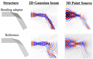
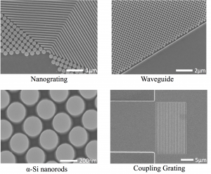
Transformation optics has inspired numerous conceptual devices since the first theoretical model of invisibility cloaks[],[]. However, the transition of these concepts into industrial applications is now widely acknowledged as a challenging bottleneck. A practical design strategy that can be adopted by industrial engineers is thus desirable at this stage. Here we propose an integrated design strategy imposing practical constraints on the area-preserving affine coordinate transformation as a general practical method to solve the problem of nonmagnetism. Practical concerns related to fabrication such as anisotropy degree and bending angles serve as additional constraints to the transformation. More details about the derivation and simulation can be found in[]. In Figure 1, we simulate the light propagating in the waveguide with or without bending adapter using finite difference time domain (FDTD) software. Obviously, the field distribution of the propagating light makes a 60° turn by the proposed bending adapter compared to a reference. In addition, Figure 2 shows the fabrication results of the bending adapter using electron beam lithography and reactive ion etching (RIE)[]. Ongoing work will focus on characterizing the adapter’s performance based on a near-field scanning optical microscope. In conclusion, we not only illustrate how to apply this practical strategy to the design of a two-dimensional electromagnetic waveguide bending adapter, but also fabricate the device for the verification. Our study is a significant step toward practical use of ideal transformation optics devices that can be implemented with natural dielectric materials.
-

-
Figure 1: FDTD simulations of the proposed bending adapter are compared to the reference without nanograting at the adapter region. Both 2D (infinite thickness at the direction perpendicular to the paper) and 3D (finite-height structure) cases agree with that the light is turned by 60° using the bending adapter.
-

-
Figure 2: Bending adapter consist of a 140-nm period nanograting (50% duty cycle) rotated 2.69° with respect to the horizon. The coupling grating deflects the light into a slab waveguide, and an impedance matching layer for reducing reflection at the boundary between the bending adapter and slab waveguide is created by a group of α-Si nanorods.
- Authors: J.-G Kim, H. J. Choi, K.-C. Park, R. E. Cohen, G. H. McKinley, G. Barbastathis
- Sponsorship: ISN, SMART
Inspired by natural structures in insect compound eyes, nanocone structures form an effective medium with an axial gradient in the refractive index, which leads to elimination of impedance mismatch at optical interfaces and hence suppresses Fresnel reflection[]. In the past we have shown that the functionality of these surfaces can be optimized by increasing the aspect ratio, since taller, narrow nanostructures contribute to a lower reflection coefficient[]. However, it is inevitable that the high aspect ratio of the slender cones is also detrimental to the mechanical robustness of the nanostructured surface, which is a critical barrier when developing textured substrates for real world applications. Here, we propose and then fabricate an inverted nanocone structure to create an improved biomimetic multifunctional film with greater mechanical robustness. While retaining the high aspect ratio of tapered nanostructures for enhancing the optical and wetting performance, the inverted nanocone structure also provides high mechanical robustness regardless of its aspect ratio.
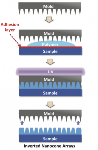
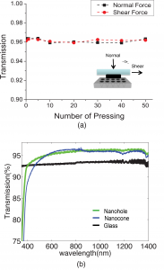
The inverted nanocone surface is fabricated using a simple UV replication method[],[] with high throughput as shown in Figure 1. A negative master mold comprising a wide area periodic array of nanoconical features was prepared using laser interference lithography ((K.-C. Park, H. J. Choi, C.-H. Chang, R. E. Cohen, G. H. McKinley, and G. Barbastathis, “Nanotextured Silica Surfaces with Robust Super-Hydrophobicity and Omnidirectional Broadband Super-Transmissivity,” ACS Nano, vol. 6 (5), pp. 3789–3799, Apr. 2012.)) in a fused silica substrate. Then it was replicated into UV curable polymer by a sequence of pressing, UV curing, and demolding steps. The fabricated inverted nanocone arrays have a pitch of 200 nm and aspect ratio of 4:1. The mechanical strength of the proposed inverted nanocone structure was quantitatively measured by applying repeated shear and normal force to the surface as shown in Figure 2 (a). Also measurements of the transmission spectra for the inverted nanocone texture were carried out in the visible to near infrared range as shown in Figure 2 (b).
-

-
Figure 1: Fabrication process of the inverted nanocone arrays replicated from nancone arrays.
-

-
Figure 2: (a) Mechanical robustness test of surfaces textured with inverted nanocone arrays. Optical transmission of the nanotextured surface after applying normal and shear force through a rubber pad. (b) Optical transmission of broadband measurement using normal incident light.
- Authors: H. J. Choi, J.-G. Kim, G. Barbastathis
- Sponsorship: Institute for Soldier Nanotechnologies
Interference lithography (IL) is one of the most effective and low-cost approaches for large-area nano-patterning and nanostructure fabrication; IL has been utilized for years to build multifunctional surfaces[], magnetic data storage media[],[], and photonic materials[],[] based on periodic nanostructures. Since it has the benefit of creating periodic structures through interference between two or more coherent laser beams, 1-dimensional (1D) grating, 2-dimensional (2D) grating, and hexagonal hole/dot arrays can be fabricated uniformly over a large area.
Although IL enables the large-scale fabrication of perfectly periodic nanostructures with rapid patterning, most of the work has been limited to creating only periodic nanostructures. In other words, aperiodic nanostructures cannot be achieved by conventional interference lithography systems such as Lloyd’s mirror interferometer and the Mach-Zehnder interferometer. Scanning beam interference lithography continuously varies the pattern period and orientation; however, it is not a simple and low-cost setup and also requires complex control devices[].
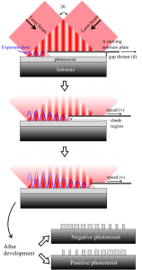
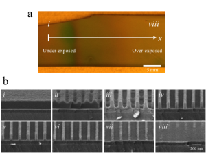
Here, we propose a novel and simple method to fabricate aperiodic subwavelength nanostructures by grayscale interference lithography (GIL) with the conventional Lloyd’s mirror interferometer and a movable aperture plate, which allows a spatially varying duty cycle of gratings with a single exposure. The proposed fabrication process for GIL is illustrated in Figure 1. The process is based on the conventional IL with exposure dose modulation by the moving aperture plate. The aperture plate can move at a speed (v) as a function of time, and exposure dose will be determined mainly by the intensity of the interfering laser beams and exposure time with the movement of the plate. Figures 2a and 2b show the image of the fabricated 1D grating sample and cross-sectional micrographs of the 200-nm period 1D grating fabricated by GID with the single exposure, respectively.
-

-
Figure 1. Schematic of GIL processes for fabricating aperiodic subwavelength nanostructures. Aperiodic subwavelength nanostructures can be created by combining conventional IL with a moving aperture plate.
-

-
Figure 2. a) Image of the subwavelength 1D grating fabricated by GIL with the single exposure. During the exposure, the aperture plate moves to the left side of the sample (-x direction) at a constant speed. b) Cross-sectional micrographs of the grating with respect to the position from i to viii regions marked in Figure 2a.
