Fabrication of Aperiodic Subwavelength Nanostructures by Grayscale Interference Lithography (GIL)
- Category: Nanotechnology, Optics & Photonics
- Tags: george barbastathis, hyungryul choi
Interference lithography (IL) is one of the most effective and low-cost approaches for large-area nano-patterning and nanostructure fabrication; IL has been utilized for years to build multifunctional surfaces[1], magnetic data storage media[2],[3], and photonic materials[4],[5] based on periodic nanostructures. Since it has the benefit of creating periodic structures through interference between two or more coherent laser beams, 1-dimensional (1D) grating, 2-dimensional (2D) grating, and hexagonal hole/dot arrays can be fabricated uniformly over a large area.
Although IL enables the large-scale fabrication of perfectly periodic nanostructures with rapid patterning, most of the work has been limited to creating only periodic nanostructures. In other words, aperiodic nanostructures cannot be achieved by conventional interference lithography systems such as Lloyd’s mirror interferometer and the Mach-Zehnder interferometer. Scanning beam interference lithography continuously varies the pattern period and orientation; however, it is not a simple and low-cost setup and also requires complex control devices[6].
Here, we propose a novel and simple method to fabricate aperiodic subwavelength nanostructures by grayscale interference lithography (GIL) with the conventional Lloyd’s mirror interferometer and a movable aperture plate, which allows a spatially varying duty cycle of gratings with a single exposure. The proposed fabrication process for GIL is illustrated in Figure 1. The process is based on the conventional IL with exposure dose modulation by the moving aperture plate. The aperture plate can move at a speed (v) as a function of time, and exposure dose will be determined mainly by the intensity of the interfering laser beams and exposure time with the movement of the plate. Figures 2a and 2b show the image of the fabricated 1D grating sample and cross-sectional micrographs of the 200-nm period 1D grating fabricated by GID with the single exposure, respectively.
-
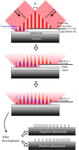
- Figure 1. Schematic of GIL processes for fabricating aperiodic subwavelength nanostructures. Aperiodic subwavelength nanostructures can be created by combining conventional IL with a moving aperture plate.
-
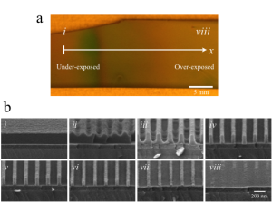
- Figure 2. a) Image of the subwavelength 1D grating fabricated by GIL with the single exposure. During the exposure, the aperture plate moves to the left side of the sample (-x direction) at a constant speed. b) Cross-sectional micrographs of the grating with respect to the position from i to viii regions marked in Figure 2a.
- K. C. Park, H. J. Choi, C. H. Chang, R. E. Cohen, G. H. McKinley, and G. Barbastathis, “Nanotextured Silica Surfaces with Robust Super-Hydrophobicity and Omnidirectional Broadband Super-Transmissivity,” ACS Nano, Apr. 8, 2012. [↩]
- M. Farhoud, J. Ferrera, A. J. Lochtefeld, T. E. Murphy, M. L. Schattenburg, J. Carter, C. A. Ross, and H. I. Smith, “Fabrication of 200 nm period nanomagnet arrays using interference lithography and a negative resist,” Journal of Vacuum Science & Technology B, vol. 17, pp. 3182-3185, Nov-Dec 1999. [↩]
- M. A. M. Haast, J. R. Schuurhuis, L. Abelmann, J. C. Lodder, and T. J. Popma, “Reversal mechanism of submicron patterned CoNi/Pt multilayers,” IEEE Transactions on Magnetics, vol. 34, pp. 1006-1008, July 1998. [↩]
- M. Campbell, D. N. Sharp, M. T. Harrison, R. G. Denning, and A. J. Turberfield, “Fabrication of photonic crystals for the visible spectrum by holographic lithography,” Nature, vol. 404, pp. 53-56, Mar 2 2000. [↩]
- C. K. Ullal, M. Maldovan, E. L. Thomas, G. Chen, Y. J. Han, and S. Yang, “Photonic crystals through holographic lithography: Simple cubic, diamond-like, and gyroid-like structures,” Applied Physics Letters, vol. 84, pp. 5434-5436, June 28 2004. [↩]
- C. G. Chen, P. T. Konkola, R. K. Heilmann, C. Joo, and M. L. Schattenburg, “Nanometer-accurate grating fabrication with scanning beam interference lithography,” Nano- and Microtechnology: Materials, Processes, Packaging, and Systems, vol. 4936, pp. 126-134, 2002. [↩]