Fabrication of Si Nanowire-Based Capacitors for Power Management
- Category: Nanotechnology
- Tags: carl thompson, wen zheng
Capacitors with high capacitance density (capacitance per footprint area) have potential applications in autonomous microsystems and for power management in high performance integrated circuits. Introducing high surface-to-volume ratio structures has been demonstrated as an effective way to increase the electrode area and therefore to improve the capacitance density. We are investigating the use of arrays of silicon nanowires for this function.
In earlier work, we demonstrated the feasibility of using metal catalyzed etching (MCE) to fabricate Si nanowires to make on-chip capacitors (Figure 1)[1]. MCE is a room temperature wet etching process that has been used to create arrays of nanowires with radii and spacing in the range of tens of nanometers, with wire aspect ratios of over 200 to 1[2]. We have demonstrated a factor of approximately 10 times improvement in the capacitance density over planar devices for nanocapacitors with a 200-nm period and 1.5-μm height.
Our current work is focused on improving the capacitor performance by decreasing the equivalent series resistance. Lower resistance will provide a higher AC effective capacitance density and less heat generation. However, we found that starting with a heavily doped substrate leads to formation of porous silicon nanowire structures, instead of solid single crystalline nanowires from lightly doped substrate (Figure 2). The porous nanowires have low conductivities and will be inappropriate for this application. Therefore, we have been looking for alternative ways to reduce the series resistance. One is starting with an epitaxial wafer that has a lightly doped epitaxial layer on top of a heavily doped bulk. After MCE, solid and single crystalline arrays of lightly doped nanowires on top of a heavily doped substrate will be generated. Another approach is to develop a post-MCE doping process to increase the doping level in lightly doped solid nanowires, which will produce solid but heavily doped nanowires. The last approach is conversion of silicon nanowires to silicide nanowires. Also, in studies of the mechanism of MCE we have found that external electric fields can affect porosity[3].
-
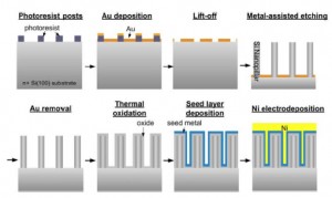
- Figure 1: Schematic nanocapacitor fabrication process flow.
-
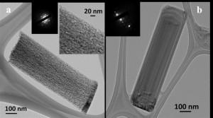
- Figure 2: TEM and SAED of silicon nanowires generated from (a) heavily and (b) lightly doped substrates by MCE.
- S. W. Chang, J. Oh, S. T. Boles, and C. V. Thompson, “Fabrication of silicon nanopillar-based nanocapacitor arrays,” Applied Physics Letters 96, 153108 (2010). [↩]
- S.W. Chang, V. P. Chuang, S. T. Boles, C. A. Ross, and C. V. Thompson, “Densely-packed arrays of ultrahigh-aspect-ratio silicon nanowire fabricated using block copolymer lithography and metal-assisted etching,” Advanced Functional Materials 19, 2495 (2009). [↩]
- P.. Lianto, S. Yu, J. Wu, C.V. Thompson, and W. K. Choi, “Vertical etching with isolated catalysts in metal-assisted chemical etching of silicon,” Nanoscale 4(23), 7532-7539 (2012). [↩]