Erbium Silicon Photonic Integrated Oscillators and Radar (ESPIOR)
- Category: Circuits & Systems
- Tags: jonathan leu, vladimir stojanovic
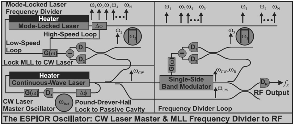
A novel device, erbium silicon photonic integrated oscillators and radar (ESPIOR), is composed of state-of-the-art silicon photonics and erbium-ytterbium based laser oscillators, integrated onto a CMOS wafer with 1fF capacitance 3D vias[1], in conjunction with hybrid attached optical components including a pump laser, an optical isolator, and a saturable absorber. ESPIOR uses a unique combination of a low phase noise continuous-wave (CW) distributed feedback (DFB) laser master oscillator, and a mode-locked laser (MLL) frequency divider to achieve a low phase noise 20-GHz microwave carrier. A schematic of the complete system is shown in figure 1.
To implement the design across the photonic wafer and CMOS wafer, a merged design environment was created. Photonic devices were drawn as parameterized cells and then treated as macro blocks that could be placed throughout the chip using scripts. For verification, design rules were added to ensure the manufacturing yield of the 3D vias that connect the circuits with the photonic devices. Layout-vs-schematic (LVS) rules were used to compare the netlist including photonic components to the integrated layout, where each contact of the photonic devices was labeled.
To test the individual photonic/electric building blocks of the ESPIOR, we have test sites for photodiodes connected with transimpedance amplifiers, linear modulators and phase shifters connected to driver circuits, switches, lasers, etc. Many combinations of design types were implemented, enabling us to test the performance tradeoffs in various designs. For instance, the driver circuit for the linear modulator was designed at different bandwidth specifications. Also, the modulator itself has travelling wave vs. lumped capacitance variants. As a demonstration of the integrated platform separate from the ESPIOR, a digital CMOS section was implemented; in it, many modulators, switches and photodiodes are connected in various link configurations. The analog CMOS transmitter and receiver frontends are highly configurable and can perform on-chip bit-error-rate testing.

Figure 1: A diagram of the ESPIOR oscillator, which utilizes the low phase noise properties of a continuous-wave laser as a master oscillator and a mode-locked laser as a frequency divider.
- C. L. Chen, D.-R. Yost, et al., “Wafer-scale 3D integration of InGaAs photodiode arrays with Si readout circuits by oxide bonding and through-oxide vias,” Microelectronic Engineering, vol. 88, no. 1, Jan. 2011. [↩]