Design and Fabrication of a Si Sub-cell for Multi-junction GaAsP/Si Solar Cells
- Category: Energy
- Tags: evelina polyzoeva, judy l hoyt
This work is part of a collaborative program aimed at ultimately achieving photovoltaic conversion with more than 40% efficiency at a lower cost by combining low-cost manufacturing on large-area Si wafers with high-efficiency III-V materials in a tandem cell. The goal of work described here is to develop a fabrication process for a tandem GaAsP/Si solar cell and silicon sub-cell and to understand the effects of the material quality on the cell performance. In the initial work, the focus is on optimizing the base Si cell to achieve the highest possible short-circuit current as it is recognized that the current from the Si sub-cell will most likely be the limiting factor in the overall performance of the tandem cell.
The Si cell process flow and device cross-section are shown in Figure 1. The doping level of the epitaxially-grown Si emitter was varied between 6×1018 cm-3 and 2.5×1019 cm-3 with a thickness between 0.25 and 1 μm. An additional 1-μm-thick boron-doped layer was grown prior to emitter growth on one of the wafers to effectively move the PN junction away from the epi-substrate interface and from possible defects. The devices with this layer present showed 10x less leakage current than the devices from wafers with emitters grown directly on the substrate. Maximum EQE of 17% and a short-circuit current density of 34 mA/cm2 (at AM1.5) was measured for the cell with emitter doping and thickness of 6×1018 cm-3 and 1 μm, respectively. The I-V characteristics are shown in Figure 2. Work is in progress on the III-V integration with these baseline Si cells.
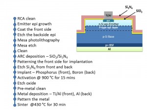
- Figure 1: Process flow and cross-section of the silicon solar cell.
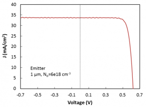
- Figure 2: I-V characteristics of a Si cell with emitter thickness of 1 μm and doping level of 6×1018 cm-3, at AM1.5.