Gate-last Process for Strained-Ge p-MOSFETs with a High-k/Metal Gate Stack
Strained-Ge MOSFETs with significantly enhanced mobility compared to Si/SiO2 hole mobility have previously been reported by our group (see Figure 1). To enable use of these enhanced channel materials in future nanoscale gate-length FETs, the equivalent oxide thickness (EOT) must be scaled, and improved dielectric/semiconductor interface properties are required. In the search for suitable gate dielectrics for use with Ge, bilayer dielectric systems have been investigated. The bottom layer in these systems is expected to provide a high-quality interface to the semiconductor while the top layer is a high-k dielectric used to reduce the overall EOT and gate leakage of the structure. An Al2O3/TiO2 dielectric system with a sub-nm EOT and low density of interface states on bulk Ge wafers has been demonstrated [1] , and its implementation with strained-Ge devices is the aim of this work. Due to the limited thermal budget associated with the bilayer dielectric/metal gate stack, a gate-last process is developed.
In the gate-last process, the source and drain regions are activated before the gate dielectric and gate metal are deposited. This is done to improve device reliability and mobility at scaled EOT, which can be significantly degraded when the high-k dielectric has gone through the high-temperature steps. Figure 2 shows the schematic gate-last process flow as well as the mask layout of the designed MOSFET structure. The preliminary experiments on gate-last Si MOSFETs show a superior interface quality compared to gate-first devices, a promising result in favor of gate-last strained-Ge MOSFETs, at least as a means of studying the dielectric/semiconductor interface.
-
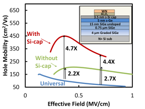
- Figure 1: Hole mobility of previously fabricated strained-Ge devices with and without a Si cap with enhancement factors up to 4.7x compared to universal Si/SiO2 hole mobility. The inset shows the cross section of the capped device. An increase in the enhancement factor is expected for an improved dielectric/semiconductor interface offered by the bilayer dielectric system.

-
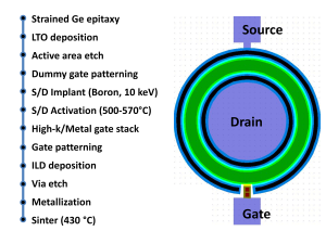
- Figure 2: Schematic gate-last process flow and mask layout of the MOSFET structure. The S/D regions are activated prior to gate dielectric/metal gate deposition to avoid high-k degradation during the high-temperature step.

- S. Swaminathan. M. Shandalov, Y. Oshima, and P. C. McIntyre, “Bilayer metal oxide gate insulators for scaled Ge-channel metal-oxide-semiconductor devices,” Applied Physics Letters, vol. 96, no. 8, pp. 082904-082904-3, Feb. 2010. [↩]