Synthesis of Monolayer Hexagonal Boron Nitride on Cu Foil using Chemical Vapor Deposition
Hexagonal boron nitride (h-BN) is very attractive for many applications, particularly as a protective coating, dielectric layer/substrate, transparent membrane, or deep ultraviolet emitter. In this work, we carried out a detailed investigation of h-BN synthesis on Cu substrate using chemical vapor deposition (CVD) with two heating zones under low pressure (LP). Previous atmospheric pressure (AP) CVD syntheses were able to obtain only a few layers of h-BN without a good control on the number of layers [1] [2] . In contrast, under LPCVD growth, monolayer h-BN was synthesized, and time-dependent growth was investigated (Figure 1). It was also observed that the morphology of the Cu surface affects the location and density of the h-BN nucleation (Figure 2). Ammonia borane, which is easily accessible and more stable under ambient conditions than borazine, is used as a BN precursor. The h-BN films are characterized by atomic force microscopy, transmission electron microscopy and electron energy loss spectroscopy analyses. Our results suggest that the growth here occurs via surface-mediated growth, which is similar to graphene growth on Cu under LP. These atomically thin layers are particularly attractive for use as atomic membranes or dielectric layers/substrates for graphene devices [3] .
-
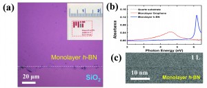
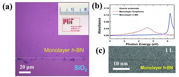
- Figure 1: Monolayer h-BN characterization. (a) Optical image of h-BN on 300 nm SiO2/Si. White dotted line indicates the border between h-BN and SiO2. The inset displays a photograph of h-BN film on a quartz substrate (red dotted area). (b) Optical absorption spectra of a monolayer h-BN, monolayer graphene and a quartz substrate (as a reference). (c) TEM image of the folded edge of a monolayer h-BN.
-
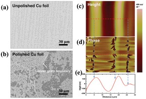
- Figure 2: Effect of copper surface morphology on h-BN growth. SEM images of (a) an unpolished copper foil and (b) a polished copper foil after h-BN growth for 10 min with T1=70 oC. (c)-(d) AFM images of the unpolished copper foil after growth: (c) height and (d) phase images. (e) Height profile along the red dotted in (c) and (d).

- Y. Shi, C. Hamsen, X. Jia, K. K. Kim, A. Reina, M. Hofmann, A. L. Hsu, K. Zhang, H. Li, Z.-Y. Juang, M. S. Dresselhaus, L.-J. Li, and J. Kong, “Synthesis of few-layer hexagonal boron nitride thin film by chemical vapor deposition,” Nano Letters, vol. 10, pp. 4134-4139, Oct. 2010. [↩]
- L. Song, L. Ci, H. Lu, P. B. Sorokin, C. Jin, J. Ni, A. G. Kvashnin, D. G. Kvashnin, J. Lou, B. I. Yakobson, and P. M. Ajayan, “Large scale growth and characterization of atomic hexagonal boron nitride layers,” Nano Letters, vol. 10, pp. 3209-15, Aug. 2010. [↩]
- K. K. Kim, A. Hsu, X. Jia, S. M. Kim, Y. Shi, M. Hofmann, D. Nezich, J. F. Rodriguez-Nieva, M. Dresselhaus, T. Palacios, and J. Kong, “Synthesis of monolayer hexagonal boron nitride on Cu foil using chemical vapor deposition,” Nano Letters, vol. 12, pp. 161-166, Jan. 2012. [↩]