- Authors: S. Bandyopadhyay, F. Yaul, A. P. Chandrakasan
- Sponsorship: MIT GaN Energy Initiative
This work focuses on using gallium nitride (GaN) FETs for an LED lighting system. The idea is to utilize the favorable figure of merit provided by the GaN technology to miniaturize the magnetic components in the power converter by using high switching frequencies for the power converter. An LED driver application is chosen because the lighting industry is expected to see substantial growth in the near future with the advent of high-efficiency LEDs. This project will demonstrate a high-efficiency, small form factor LED lighting system with a long lifetime that can replace incandescent bulbs or CFLs. Efforts aim for design and implementation of high power density, off-line, high-frequency power conversion and control circuits.
The drivers are being implemented on a CMOS die. This will directly interface with discrete commercial GaN power devices. Circuits to perform power factor correction and dimming control are also being designed. Since the system will interface directly with the AC mains, an EMI filter is being used with the rectifier. Figure 1 shows the high-level block diagram of the system envisioned.

Figure 1: Block diagram of LED driver.
- Authors: D. S. Lee, E. Matioli, T. Palacios
- Sponsorship: DARPA NEXT Program, NSF CAREER Award, ONR DURIP Program
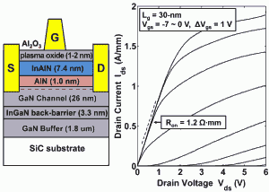
The unique combination of high electron velocity and high breakdown voltage of GaN makes this material an ideal candidate for high power and high frequency applications. Among the different possible nitride structures, an InAlN/GaN heterostructure is one of the most promising candidates for high frequency applications because the large polarization discontinuity between InAlN and GaN induces an extremely large charge density with barriers thinner than 10 nm.
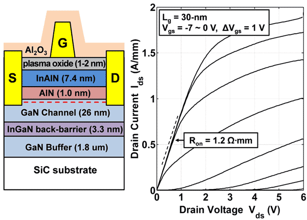
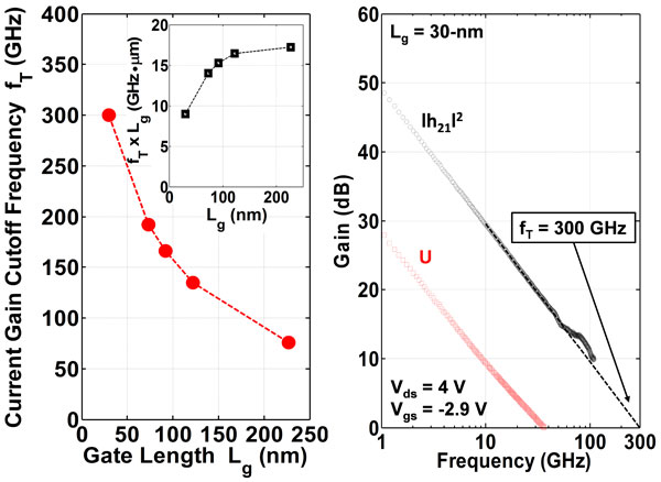
This work reports lattice-matched In0.17Al0.83N/GaN high electron mobility transistors (HEMTs) on a SiC substrate with a record current gain cutoff frequency (fT) of 300 GHz [1-2]. To suppress short-channel effects (SCEs), an In0.15Ga0.85N back-barrier is applied in an InAlN/GaN heterostructure for the first time. The GaN channel thickness is also reduced to 26 nm, which allows a good immunity to SCEs for gate lengths down to 70 nm, even with a relatively thick top barrier (9.4-10.4 nm). In a device with a gate length (Lg) of 30 nm, an on-resistance (Ron) of 1.2 Ω•mm, and an extrinsic transconductance (gm.ext) of 530 mS/mm, a peak fT of 300 GHz is achieved. An electron velocity of 1.37-1.45×107 cm/s is extracted by two different delay analysis methods.
-
-
Figure 1: (a) Cross-sectional schematic of an InAlN/GaN HEMT with an InGaN back-barrier. (b) Ids-Vds characteristics of the devices with Lg = 30 nm.
-

- Authors: Z. Liu, T. Palacios
- Sponsorship: Singapore-MIT Alliance for Research and Technology
GaN is an excellent material to be used in high-power, high-frequency and high-temperature applications due to its wide band gap, high saturation velocity, etc. The monolithic integration of GaN power and/or high frequency devices with Si CMOS digital ICs would enable a new level of circuit design flexibility [] . However, typically the GaN device fabrication uses different process technologies from the standard CMOS technologies in Si foundries, such as the Au-contained ohmic process. To realize the target of GaN and Si CMOS integration, Si-CMOS compatible process technologies need to be developed. For the first step, we endeavor to find an Au-free ohmic contact recipe with low contact resistance and smooth metal surface.
The samples we used in this work have a 3-nm GaN cap, a 20-nm unintentionally doped AlGaN barrier layer, and a GaN buffer layer grown on a 6-inch Si wafer. Mesa isolation was realized using ICP systems with Cl2/BCl3 gases. For the ohmic contact, we tried different metal schemes including Ti/Al, Ti/Al/Ti, Ti/Al/Pt, Ti/Al/Ni/Pt, Ti/Ge/Ti/Al/Ni/Pt, Si/Ti/Al/Ti/Ta, Mo/Al/Mo/Ti, Ta/Al/Ta, Ta/Al/Ni/Ta, etc, with different annealing temperatures varying from 500°C to 975°C using rapid thermal annealing (RTA) in N2 ambience. We also tried to include a shallow recess using low etch-rate SiCl4 plasma etch in an ICP system to improve the ohmic contact. Among these recipes, the metal scheme of Ti/Al/Ni/Pt is found to give a relatively low contact resistance with very good metal surface. Lower ohmic contact resistance values together with a smooth metal surface can be obtained if a 20-30-nm recess is added.
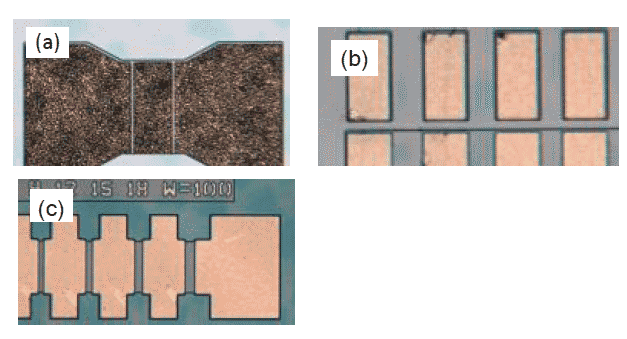
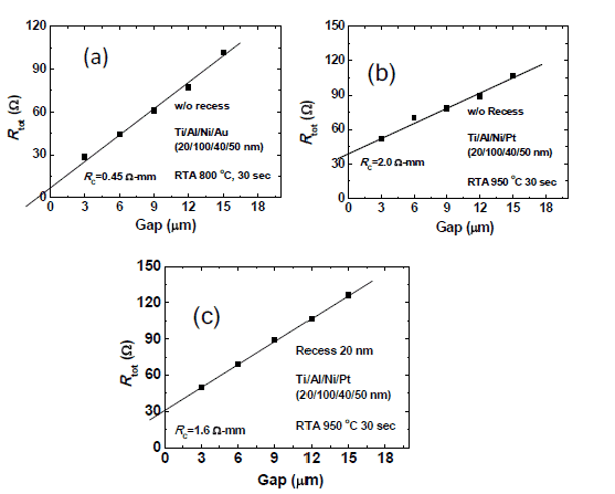
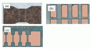
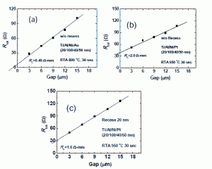
Figure 1 shows the optical pictures of the ohmic metal surface after RTA for 30 s for metal schemes of Ti/Al/Ni/Au, Ti/Al/Ni/Pt, and Ti/Al/Ni/Pt with recess. The Au-contained recipe shows a very rough surface even it is annealed at a relatively low temperature of 800°C. The intermixing of Al and Au and the formation of viscous AlAu4 phase are believed to result in the rough surface [] . Without Au, the metal surface of Ti/Al/Ni/Pt is very smooth even it is annealed at a much high temperature up to 950°C. The recess of 20 nm (and 30 nm, not shown here) has no obvious effect on the metal surface after annealing. Figure 2 shows the typical contact resistance (RC) values measured using the transition length method (TLM). A low RC of around 0.45 Ω-mm can be obtained for the normal Ti/Al/Ni/Au recipe. The RC value of Ti/Al/Ni/Pt metal is higher (~2.0 Ω-mm), and it can decrease to 1.6Ω-mm with the recess of 20 nm. In the future, more work needs to be carried out to further lower the RC and optimize the Au-free ohmic contact recipes.
-
-
Figure 1: The optical pictures of ohmic metal surfaces for AlGaN/GaN HEMTs. (a) Ti/Al/Ni/Au with RTA at 800°C; (b) Ti/Al/Ni/Pt with RTA at 950°C; and (c) Ti/Al/Ni/Pt with 20-nm recess and RTA at 950°C.
-
-
Figure 2: TLM results of the ohmic contact for AlGaN/GaN HEMTs. (a) Ti/Al/Ni/Au with RTA at 800°C; (b) Ti/Al/Ni/Pt with RTA at 950°C; and (c) Ti/Al/Ni/Pt with 20-nm recess and RTA at 950°.
- Authors: D. Piedra, B. Lu, M. Sun, E. Matioli, H.-S. Lee, T. Palacios
- Sponsorship: MIT GaN Energy Center, ARPA-E ADEPT, DOE GIGA, SRC/FCRP MSD, SRC/FCRP IFC
Wide band-gap III-nitride semiconductors have great potential for the next generation of power electronics. GaN high-electron-mobility transistors (HEMTs) in particular have attracted great interest due to their high breakdown electric field and high electron mobility. With lower conduction loss and higher switching frequency, GaN-based transistors can improve the efficiency and reduce the size of many power electronics systems.
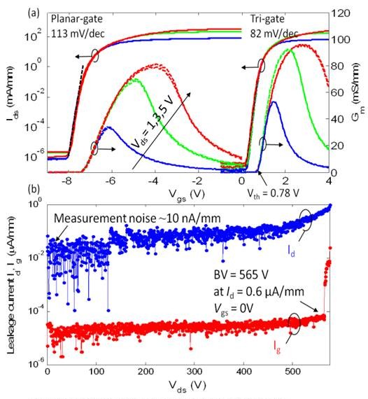
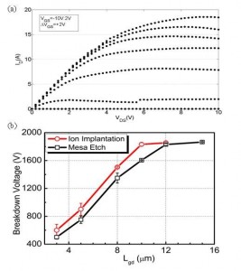
The standard AlGaN/GaN HEMTs are depletion-mode transistors. However, normally-off transistors are preferred in power electronics. Recently, our group has developed a new normally-off tri-gate GaN metal-insulator-semiconductor-field-effect-transistor (MISFET) [] . By using a three-dimensional tri-gate structure and a sub-micron gate recess, we achieve high performance normally-off GaN transistors with a breakdown voltage as high as 565 V at a drain leakage current of 0.6 μA/mm. The new tri-gate normally-off GaN MISFET has a maximum current density of 530 mA/mm and an on/off current ratio of more than 8 orders of magnitude with a sub-threshold slope of 86±9 mV/decade, as Figure 1 shows. We have also demonstrated a new multi-finger technology with higher yield and lower device resistance for InAlN/GaN HEMTs. A multi-finger device with gate width of 39.6 mm has an on-resistance (Ron) of 0.244 Ω and a maximum current of 18.5 A, as in Figure 2(a).
Finally, ion-implantation isolation technology has also been developed. A state-of-the-art 1800 V breakdown voltage with 2.2 mΩcm2 specific on-resistance has been achieved on AlGaN/GaN HEMTs on Si substrate (Figure 2(b)). Devices with ion-implantation isolation have higher breakdown voltage than devices using mesa-etching isolation, showing that ion-implantation isolation is a promising candidate for the next-generation high voltage GaN-based HEMT fabrication.
-

-
Figure 1: (a) Transfer characteristics of a tri-gate normally-off GaN MISFET and a standard planar-gate D-mode GaN MIS-HEMT. Both devices have Lgs = 1.5 μm, Lg = 2 μm, Lgd = 10 μm and W = 100 μm. (b) Three-terminal breakdown voltage (BV) measurement of the tri-gate normally-off GaN MISFET with Lgd = 10 μm at Vgs = 0 V.
-
-
Figure 2: (a) Id-Vd characteristic of a multifinger device with Wg = 39.6 mm and Ron = 0.244 Ω. (b) Three-terminal breakdown voltage as a function of Lgd for implantation and mesa devices. The inset shows the breakdown voltage at leakage current of 10 μA/mm
- Authors: S. C. Tan, F. Gao, J. Joh, L. Li, T. Palacios, J. A. del Alamo, C. V. Thompson, S. C. Tan, F. Gao, J. Joh, L. Li, T. Palacios, J. A. del Alamo, C. V. Thompson
There is an increasing interest in AlGaN/GaN high electron mobility transistors (HEMTs) due to their great potential for high performance at microwave frequencies. However, the performance of these devices is often limited by material reliability issues. Unfortunately, a detailed physical understanding of the degradation mechanisms is still lacking. The objective of this project is to develop that understanding through appropriate testing and failure analysis, so that test methods and models can be developed that will lead to further improvement in the reliability and electrical performance of these devices though optimization their design.

Figure 1: Pits and particles observed at the gate edges of a stressed AlGaN HEMT (top view) [] .
Recent work has focused on the formation of pits at the edge of the gate contact during electrical stressing and performance degradation [] [] [] . These pits have been observed to form under a variety of stressing conditions and in a range of temperatures. We have found that in some cases the pits are associated with formation of particles that appear to be an oxide of Ga (Figure 1), and that pit and particle formation is suppressed when samples are properly passivated or when they are stressed in ultra-high vacuum conditions. Also, stressing in the presence of water vapor was found to enhance the rate of degradation [] . This suggests that this failure mechanism is associated with electrochemically-enhanced oxidation. We have also observed that the rate of pit formation is affected by temperature, both in isothermal experiments and in experiments in which the temperature within an individual device varies significantly. This finding indicates that this failure process is thermally activated. We estimate an activation energy of about 0.3eV [] .
Analytical techniques such as scanning electron microscopy (SEM), transmission electron microscopy (TEM), atomic force microscopy (AFM), cathode luminescence (CL), and energy-dispersive X-ray spectroscopy (EDX) will be employed in future studies of this and other degradation processes, with the goal of developing predictive models for failure rates and reliability.
- Authors: M. Azize, O. I. Saadat, T. Palacios
- Sponsorship: ONR, NSF
Nitride transistors with current gain cut-off frequencies (fT) of 300 GHz and power gain cut-off frequencies (fmax) of 394 GHz have been reported [] [] . However, the frequency performance of these devices is still far from the theoretical limit due to poor gate modulation efficiency, short channel effects, high access resistances (Ra), and specific contact resistance (rc). Nanoribbon (NR)-based nitride HEMTs could overcome many of these limitations by improving the electron confinement thanks to the excellent electrostatics of wrap-around gates [] . Moreover, strong piezoelectric-induced doping can be generated in NR nitride-based semiconductors and increase the maximum operating frequency of nitride devices by reducing the parasitic resistances (Ra and rc). In this project, we study the use of Ti-induced strain in InAlN/GaN NR HEMTs.
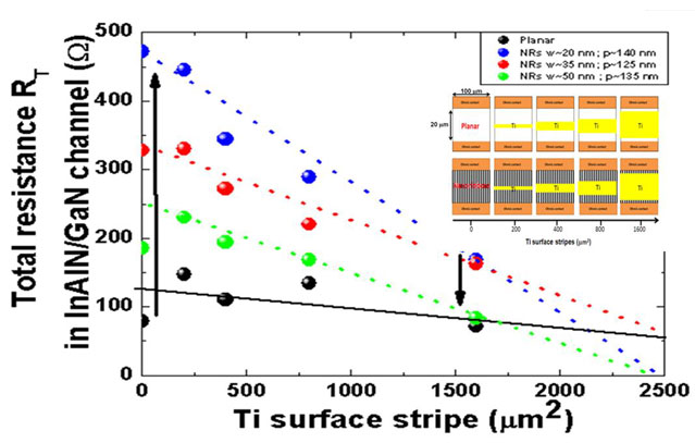
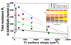
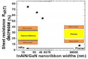
NR and planar devices are fabricated on the same chip. A Ti/Al/Ni/Au metal stack is then deposited for ohmic contact formation. Electron beam lithography and dry etching are performed in some devices to define NR structures between the ohmic contacts with widths (w) in the w~20-90 ± 10 nm range and a period (p) of p~135 ± 10 nm. An additional Ti strip was deposited between the ohmic contacts (cf. inset of Figure 2) with a width of ~100 mm and a length varying from ~2 to 16 mm and annealed at 870 ◦C for 30 s in N2 environment. Figure 1 shows the total resistance RT in NR and planar devicesas a function of the area coverage of the Ti stripes. A quasi-linear RT decrease is observed when the Ti surface area increases in the InAlN/GaN NRs samples, unlike in the planar device. The mechanical stress introduced by Ti stripes has a strong effect on the transport properties of InAlN/GaN NRs. Figure 2 shows the decrease of the sheet resistance (RshTi) underneath the Ti stripe in InAlN/GaN NRs as a function of NR widths. The RshTi in the NR and planar devices is decreased by ~50-75 % and ~10%, respectively.
-
-
Figure 1: Total resistance in InAlN/GaN channel as a function of the area coverage of the Ti stripes. The inset shows a cartoon of NR and planar devices with different area coverage of the Ti stripes.
-
-
Figure 2: Sheet resistance underneath of the Ti metal stripes in InAlN/GaN devices as a function of the NR width. The inset shows a cartoon of NR and planar devices with identical area coverage of the Ti stripes.
- Authors: F. Gao, S. Keller, U. K. Mishra, C. V. Thompson, T. Palacios
- Sponsorship: ONR DRIFT-MURI
Thanks to their excellent electrical performance, AlGaN/GaN high electron mobility transistors (HEMTs) are considered ideal devices for the next generation of high-power and high-frequency electronics [] . However, the limited understanding of their long-term reliability and degradation mechanisms is slowing down the insertion of these devices in actual systems [] .
Recently, we have reported the formation of oxide particles next to the gate edge of GaN HEMTs after OFF-state step-stress degradation experiments [] . Underneath these particles, pits similar to the ones reported in previous papers [] are observed. In this work, we investigate the role of oxygen in the formation of these particles/pits during OFF-state stress and use oxygen diffusion barriers to improve the reliability of AlGaN/GaN HEMTs.
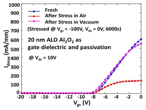
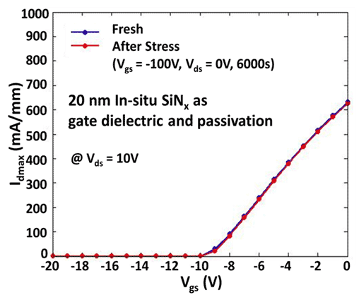
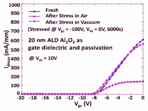
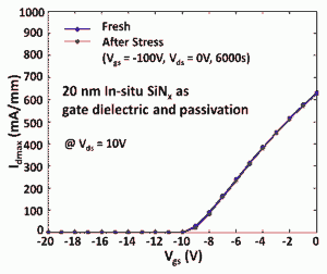
Two different dielectrics have been used: Al2O3 deposited by atomic layer deposition and in-situ SiNx deposited immediately after the growth of the AlGaN/GaN epitaxial layer by metal organic chemical vapor deposition (MOCVD). Step-stress degradation experiments were performed in both samples in air and vacuum. No degradation was found in either sample during the experiments in vacuum, which shows that the oxygen necessary for the particle formation probably comes from air. In contrast, when the samples were stressed in air, a large degradation and particle/pit formation were found in the Al2O3-passivated sample, while no structural or electrical degradation was found in the sample with in-situ SiNx (see Figures 1 and 2). The in-situ SiNx dielectric is believed to be a much better diffusion barrier for oxygen gas and water vapor than Al2O3, which significantly reduces device degradation.
In summary, the in-situ deposition of a SiNx gate dielectric and passivation layer successfully eliminated the diffusion of oxygen from air and water vapor to the AlGaN surface, which improved the OFF-state reliability of AlGaN/GaN HEMTs.
-
-
Figure 1: Transfer characteristics of the device with ALD Al2O3 gate dielectric stressed at Vgs = -100 V and Vds = 0 V for 6000 s in air and in vacuum. Permanent degradation of the drain current is observed in air.
-
-
Figure 2: Transfer characteristics of the device with in-situ SiNx gate dielectric stressed at Vgs = -100 V and Vds = 0 V for 6000 s in air. No current degradation is observed.