- Authors: R.M. Iutzi, E.A. Fitzgerald
- Sponsorship: NSF Center for Energy Efficient Electronics Science (E3S)
Tunnelling devices based on semiconductor heterojunctions offer the potential for computation with very high energy efficiency. This potential exists because devices that utilize quantum tunnelling as a switching mechanism are not limited in the sharpness of their turn-on, in contrast to thermally activated devices such as MOSFETs, whose turn-on is limited due to a minimum possible subthreshold slope of 60 mV/decade. In the past few years, much work has focused on InAs/AlGaSb heterojunctions [] due to their type-III band alignment. While simulations have shown the potential for excellent subthreshold slopes, there has been limited experimental work to date to determine if these devices can actually achieve strong performance in light of the many materials aspects that cannot be accounted for in simulation.
Our work focuses on understanding the materials properties of tunnelling heterojunctions, how they affect device performance, how they can be controlled from a processing perspective, and how they affect device performance. Specifically, we are exploring the various defects present in InAs/AlGaSb heterojunctions and how they can be minimized. We have found that these structures are highly sensitive to the nature of the interface, with certain interface types leading to metallic structures that inhibit growth or significant dislocation densities, which may weaken device performance. We have developed techniques to minimize these defects.
Additionally, we are exploring alternatives to Sb-based devices; specifically heterojunctions utilizing InAs and Ge. We have developed processes to epitaxiallly grow these materials together with varying Ge dimensionalities including 0D (Ge quantum dots), 1D (Ge nanowires), and 2D/3D (Ge thin film). We are currently assessing the various materials defects present in these highly-strained structures, such as dislocations and stacking faults, and how they affect device performance.
-
-
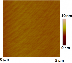
Figure 1: Atomic force microscopy (AFM) image of epitaxially regrown GaSb, with atomic steps apparent on the surface and no defects.
-

-
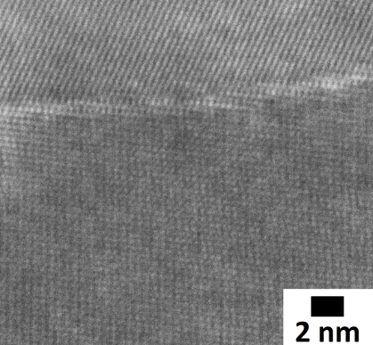
Figure 2: Lattice-resolved transmission electron microscopy (TEM) image of Ge grown on top of a (100) InAs surface, offcut 6° towards (110), with (100) facets visible.
- Authors: A. Jandl, M. Bulsara, E. A. Fitzgerald
- Sponsorship: Solid State Solar Thermal Energy Conversion Center

Figure 1: The threading dislocation density (TOP) in InAsxP1-x graded buffers does not significantly increase with higher strain gradients. The threading dislocations appear to be highly mobile with a calculated velocity of 40.9 μm/s at the growth temperature. This velocity was found by fitting the data with a least-squares regression (the “No Buffer” sample was not included). Increased strain gradients do cause a marginal increase in the RMS surface roughness (BOTTOM). RMS roughness was calculated from a 25×25 μm AFM image.
Semiconducting alloys of InxGa1-xAs, GaAsySb1-y, and InAszP1-z can be fabricated to exhibit band gaps between 0.5 and 1.0 eV, which are suitable for thermophotovoltaic (TPV) devices. However, the compositions of interest are not lattice-matched to any of the common III-V compound semiconductor substrates. Direct growth of these alloys on common substrates would result in high threading dislocation densities (TDD) in the active layers. Since TPV devices require long minority carrier lifetimes, the dislocation density needs to be minimized for efficient performance. The objective of our research is to establish robust lattice constant engineering approaches to allow broad tunability of the band gap of TPV devices. We have researched the properties of compositionally graded buffers of InAszP1-z on InP substrates to provide a platform for high quality thin films of InxGa1-xAs, GaAsySb1-y, and InAszP1-z alloys over a range of lattice constants and band gaps.
InAsxP1-x compositionally graded buffers were prepared with metal-organic chemical vapor deposition (MOCVD) system. A set of samples was fabricated to study the TDD evolution as a function of the strain gradient (% strain/µm) in the buffer. The samples consisted of graded buffers with strain gradients between 0.33 % strain/μm and 1.37 % strain/μm and final cap composition of InAs0.4P0.6. One sample included in this set was a layer of InAso.4Po.6 grown directly on InP that intentionally lacked a graded buffer. Figure 1 shows the threading dislocation density and surface roughness for this set of samples. Assuming an equilibrium strain relaxation process, we determined the dislocation glide velocity in the InAsxP1-x graded buffers to be 40.9 μm/s using a least-square fit of the data. This velocity is relatively high and allows for low dislocation densities for high strain gradients. Although surface roughness increases with strain gradient, the greatest roughness was still suitable for device processing.
- Authors: K. Mukherjee, M. T. Bulsara, E. A. Fitzgerald
- Sponsorship: National Renewable Energy Laboratory
Yellow-green LEDs with emission at the wavelengths of 570-580 nm are commercially interesting because they can be combined with blue LEDs (470-480 nm) to create energy efficient white light. More recently there has also been interest in combining yellow-green LEDs with red, green, and blue LEDs to allow for the fabrication of high-quality tunable color LEDs for commercial lighting and displays [] . Alloys of (AlxGa1-x)0.5In0.5P lattice matched to a GaAs substrate have traditionally been used to make 650-nm red LEDs (x=0) and, by increasing the aluminum/gallium ratio (x=0.4), amber LEDs at 610 nm. The efficiency of this alloy drops sharply with any further increase in aluminum/gallium as the material slowly transitions to having an indirect bandgap [] .
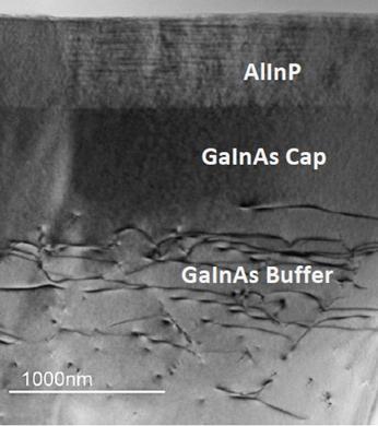
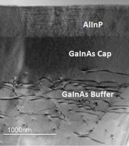
Growing AlGaInP on lattice engineered substrates, away from the GaAs lattice constant, breaks the lattice matching constraint on composition and allows for greater flexibility in moving from amber to yellow-green emission without severe reduction in efficiency [] . In this project we start out with a GaAs substrate and grow compositionally graded buffers of either GayIn1-yAs or GazAs1-zP to reach lattice constants greater or lesser than GaAs, respectively. Once the desired lattice constant is reached, AlGaInP lattice matched to the buffer is grown, and its optical properties are characterized. AlGaInP alloys are also known to exhibit CuPt-B ordering under certain growth conditions that affect the bandstructure [] . There are very limited reports on growing AlGaInP at compositions that are not lattice-matched to GaAs, so this project aims to experimentally map out the bandgap/color space and effect of ordering in this material system as well. LEDs based on lattice mismatched AlGaInP are currently being fabricated to investigate the optical quality of the film as well as the effect of dislocations on device efficiency and lifetime.
-
-
Figure 1: Cross section TEM micrograph of an Al0.35In0.65P film grown on a Ga0.8In0.2As compositionally graded buffer on a GaAs substrate. The lattice mismatch is completely relaxed via misfit dislocations in the buffer away from the AlInP film.
-
-
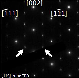
Figure 2: Electron diffraction pattern along the [110] axis of the Al0.35In0.65P film showing additional superspots (marked by arrows) at the ½[-1 1 1] and ½[1 -1 1] direction typical of CuPt-B ordering. The ordering has been shown to reduce the bandgap by more than 150meV.
- Authors: P. Sharma, M. T. Bulsara, E. A. Fitzgerald
- Sponsorship: ARO
Photovoltaics and sustainability have received much attention lately. We seek a tandem photovoltaic device using silicon as both the substrate and lower cell and GaAsP as the upper cell. The ideal band gaps for this two-cell tandem structure with silicon at 1.1eV and GaAsP at 1.75 eV allow access to the highest efficiency possible for a two-cell tandem, 36.5%. The lattice mismatch between GaP and Si is 0.37%; therefore, these two materials constitute a nearly ideal combination for the integration of Si and III–V semiconductor-based technologies. Nevertheless, defect-free heteroepitaxy of GaP on Si has been a major challenge.
One can envision a process in which a Si1-xGex graded buffer is grown on a Si wafer to extend the lattice parameter part of the way to GaAs, at which point a lattice-matched GaAsyP1-y is grown on the Si1-xGex surface, followed by tensile grading of the GaAsyP1-y until GaP is reached. Identifying the composition where the transition can be made from Si1-xGex to GaAsyP1-y depending on the application is an integral objective of this study. This identification will provide the flexibility to engineer the lattice constants from Si to Ge and GaP to GaAs while maintaining low threading dislocation density (TDD) and surface morphology suitable for device processing. This study has achieved the successful growth of high-quality lattice-matched GaAsyP1-y on Si0.5Ge0.5, Si0.4Ge0.6, and Si0.3Ge0.7 virtual substrates. Various characterization techniques clearly reveal a high-quality crystalline interface (Figure 1) between Si1-xGex and GaAsyP1-y with low TDD suitable for device processing, no rampant dislocation nucleation, anti-phase boundaries, stacking faults or other crystalline defects. Further work will explore the temperature window for the epitaxial growth of GaAsyP1-y on Si1-xGex with higher Si content, as the end goal is to obtain a defect-free GaP film on Si substrate.

Figure 1: Cross-sectionalbright field TEM of GaAsyP1-y on (a) Si0.5Ge0.5 and (b) Si0.4Ge0.6 virtual substrates on 6° offcut towards the nearest {111} plane Si (001) substrate.