Thermal Ink Jet Printing of CNT films
- Category: MEMS & BioMEMS
- Tags: phillip lee, sang-gook kim
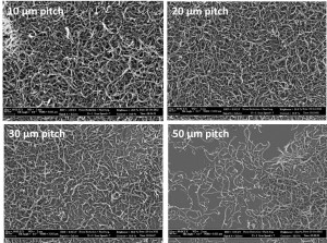
Ink jet printing allows for rapid, scalable, and low-cost patterning process. It does not need a vacuum environment or toxic etching process, which facilitates the integration of ink jet printing into other micro-machining process. And ink jet printing can pattern on curved surface or 3D structure. The characteristics of this technique are advantageous in industry. Previously, we demonstrated highly repeatable and uniform PZT thin film with ink jet printing[1],[2]. With this know-how in PZT film printing, we apply carbon nanotubes to ink jet printing. Due to their mechanical, thermal conductive and electrical properties, carbon nanotubes find diverse applications. The percolation network of carbon nanotubes is a transparent and conductive material, and strong bonding among carbon nanotubes enables fabrication of a bendable, foldable, and stretchable electrode. Previous research from other groups fabricated an ink jet-printed carbon nanotubes conductor[3], but the performance was not good enough to replace the current ITO transparent electrode. In this research, we controlled the amount of carbon nanotube deposition by changing the pitch of the printed line, which determines conductivity and transparency. Electrodes of 30% transparency can be fabricated using 10-um pitch, which has 36.6 S/cm conductivity and 247 ohm/sq sheet resistance. Increasing the pitch size up to 20 um gives the electrode properties of 74% transparency, 30.8 S/cm conductivity and 1.1 Kohm/sq sheet resistance. This result shows better performance compared with previous research. Figure 1 shows the SEM image of fabricated electrodes depending on the pitch size. Printed film shows uniformly deposited carbon nanotubes percolation network within 30- um pitch size. In the future, we plan to produce devices that utilize the full capabilities of this process to achieve better performance in both conductance and transparency, which will enable applications such as touch panels, organic light-emitting diodes, and solar cells.
- S. P. Bathurst and S. G. Kim, “Designing direct printing process for improved piezoelectric micro-devices,” CIRP Annals – Manufacturing Technology, vol. 58, pp. 193-196, 2009. [↩]
- S. P. Bathurst, H. W. Lee, and S. G. Kim, “Ink jet printing of PZT thin films for MEMS applications,” Proc. International Conference on Digital Fabrication, 2008, pp. 897-901. [↩]
- W. R. Small, F. Masdarolomoor, G. G. Wallace, and M. in het Panhuis, “Inkjet deposition and characterization of transparent conducting electroactive polyaniline composite films with a high carbon nanotube loading fraction,” Journal of Materials Chemistry, vol. 17, no. 41, pp. 4359-4361, 2007. [↩]
