Silicon Field Emission Devices for X-ray Generation
- Category: Medical Electronics, Nanotechnology
- Tags: luis velasquez-garcia, shuo cheng
This work focuses on developing an X-ray source using microfabricated silicon field emission devices. In the X-ray source, the electrons emitted from a field emission device are accelerated towards a transmission anode plate, generating x-ray (bremsstrahlung) as they decelerate upon reaching surface of the anode plate. Our goal is to fabricate a device with multiple individually addressable emitters to implement coded source imaging technique for phase contrast X-ray imaging[1]. We also need to focus the electron beams generated from each emitter to form a micron-sized interaction spot on the anode. The final device is expected to consist of arrays of silicon tips, with two gates above each of the tips. The proximal gate is for electron extraction, and the distal gate is for electron beam focusing. As a first step of testing the concept, we developed a process flow to fabricate a field emission device with only one gate. The process flow is shown in Figure 1. The fabricated devices can emit 0.2 µA of current per peak, at 75 V of gate-to-emitter extraction voltage. The device will be tested in a home-built X-ray generation facility. The facility, as shown in Figure 2, is a high vacuum (down to 2 x 10⁻⁸ Torr) chamber that provides high voltage connections to test X-ray generation functionality of our fabricated field emission devices. The facility accelerates the electrons with up to 60 kV of anode voltage and allows the generated X-ray to transmit out of the chamber through a beryllium window. Initial functionality test of the chamber using a carbon-nanotube field emitter has successfully generated X-ray image of an ex-vivo sample. We expect to generate X-ray image from our first generation silicon field emission devices in the near future.
-
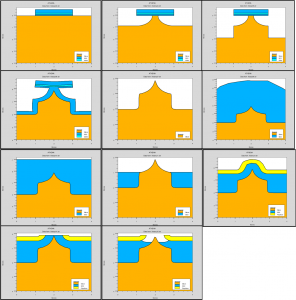
- Figure 1: Process flow of the single-gated field emission device, simulated using Silvaco.
-

- Figure 2: A picture of the X-ray generation facility.
- A. Damato, “Capabilities and limitations of Phase Contrast Imaging techniques with X-rays and neutrons,” Doctoral thesis, Massachusetts Institute of Technology, Cambridge, 2009. [↩]