Membrane-integrated Superconducting Nanowire Single-photon Detectors
- Category: Nanotechnology, Optics & Photonics
- Tags: faraz najafi, karl berggren
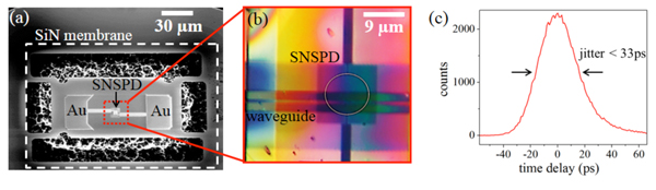
Fig. 1. (a) SEM of a SiNx membrane (~ 350-nm thick) with SNSPD on top. (b) Optical micrograph of a membrane-SNSPD that was transferred and aligned to a Si waveguide on a PIC chip. (c) Instrument response function (IRF) of a membrane-SNSPD transferred onto a secondary substrate. The IRF was measured using a mode-locked fiber-coupled laser with sub-ps-pulse-width and 1550-nm wavelength. We measured sub-35-ps timing jitter for detectors with IC > 13 μA.
Superconducting nanowire single-photon detectors (SNSPDs)[1] based on niobium nitride (NbN) nanowires have shown high speed (< 3ns dead time[2] ) and timing resolution (sub-30-ps timing jitter[3] ), making SNSPDs a leading single-photon detection technology in the near-infrared range.
Recently SNSPDs have attracted interest as components in photonic integrated circuits (PICs), which enable the generation, manipulation, and detection of non-classical photons on a single chip. Previous approaches to integrating SNSPDs with photonic structures[4][5][6] were compatible with only a handful of substrate materials and required additional fabrication steps on the sample. These steps can be incompatible with complex and delicate PICs. Based on a micron-scale flip-chip concept[7], we have developed a technology that enables integration of SNSPDs on PICs without exposing the PIC to chemicals or high temperatures. We used this method to integrate SNSPDs with silicon waveguides designed for 1550-nm center wavelength.
NbN-SNSPDs based on sub-100-nm-wide nanowires were fabricated on top of a SiNx-on-Si substrate. The underlying silicon was removed via isotropic dry etch in XeF2, resulting in SNSPDs on suspended ~350-nm-thick SiNx membranes. The scanning electron micrograph (SEM) of a membrane-SNSPD is shown in Figure 1(a). Micro-manipulated tungsten probes were used to pick up the membrane and visually align it to the waveguide on the PIC chip. Figure 1(b) shows a membrane-SNSPD after transfer onto a waveguide.
Preliminary measurements on membrane-SNSPDs that were transferred on a secondary substrate showed that the contact between the membrane and the secondary substrate was sufficient to cool the detector in a continuous-flow cryostat, where we measured sub-35-ps timing jitter, as shown in Figure 1(c). While the photonic structures demonstrated here are waveguides, this technology could be applied to other PICs that require on-chip integration and near-field single-photon detection.
- G. Gol’tsman et al., Applied Physics Letters 79, pp. 705-707 (2001); [↩]
- F. Marsili, F. Najafi, E. Dauler, R. J. Molnar, and K. K. Berggren, Applied Physics Letters 100, no. 112601 (2012); [↩]
- E. A. Dauler, B. S. Robinson, A. J. Kerman, J. K. W. Yang, K. M. Rosfjord, V. Anant, B. Voronov, G. Gol’tsman, and K. K. Berggren, IEEE Transactions on Applied Superconductivity 17, pp. 279-284 (2007); [↩]
- J. Sprengers et al., Applied Physics Letters 99, no. 181110 (2011); [↩]
- W. Pernice et al., Nature Communications 3, no. 1325 (2012); [↩]
- K. Rosfjord et al., Optics Express 14, pp. 527-534 (2006); [↩]
- D. Englund et al., U.S. Patent Application No. 13/633,647; [↩]