Large-scale Nanophotonic Phased Array
- Category: Nanotechnology, Optics & Photonics
- Tags: jie sun, michael watts
Electromagnetic phased arrays at radio frequencies (RFs) are well known and have enabled applications from communications to radar, broadcasting, and astronomy. Research has long pursued the ability to generate arbitrary radiation patterns with large-scale phased arrays. Deploying large-scale RF phased arrays is expensive and cumbersome; optical phased arrays have an advantage in that the much shorter optical wavelength holds promise for large-scale integration. However, the short optical wavelength also imposes stringent requirements on fabrication. Optical phased arrays have been studied with various platforms and even chip-scale nanophotonics, but demonstrations so far have been restricted to one-dimensional (1D) or small-scale 2D arrays.
Here[1] we demonstrate a large-scale 2D nanophotonic phased array (NPA), in which 64 × 64 (4,096) optical nanoantennas are densely integrated on a silicon chip within a 576 μm × 576 μm footprint with all nanoantennas precisely balanced in power and aligned in phase to generate a designed, sophisticated radiation pattern in the far field, as in Figure 1. We show that active phase tunability can be realized in this NPA by demonstrating dynamic beam steering and shaping with an 8 × 8 array. This work demonstrates that a robust design, together with state-of-the-art complementary metal-oxide–semiconductor (CMOS) technology, allows implementation of large-scale NPAs on compact and inexpensive nanophotonic chips. In turn, the large-scale phased aray enables arbitrary radiation pattern generation and extends the functionalities of phased arrays beyond conventional beam focusing and steering, opening possibilities for large-scale deployment in applications such as communication, laser detection, and ranging, 3D holography, among others.
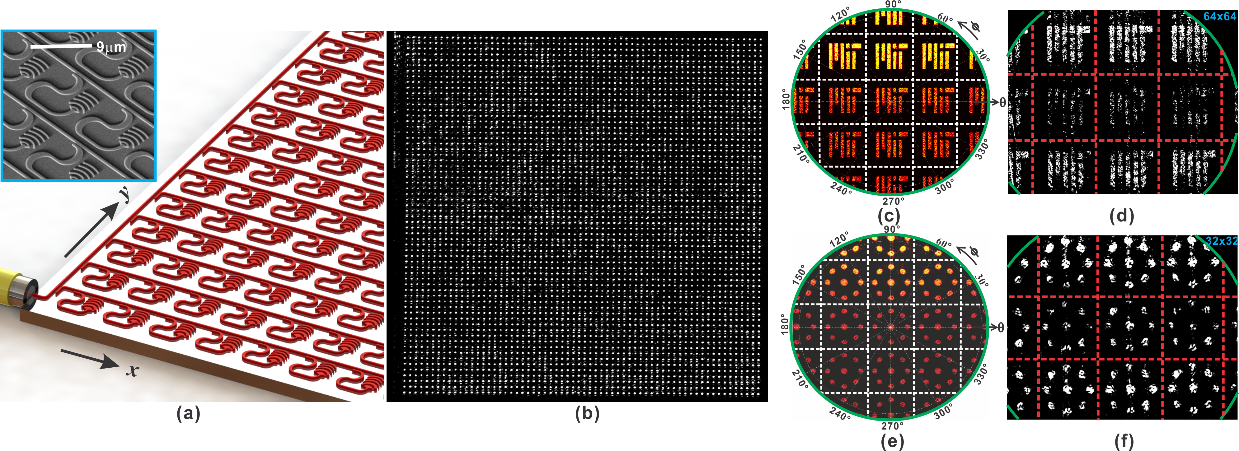
Figure 1. Passive phased arrays. (a) A schematic of the large-scale optical phased array. Inset, a scanning electron micrograph (SEM) of a part of the phased array fabricated with the state-of-the-art CMOS technology. (b) Near-field emission of a 64×64 phased array. (c) Simulated and (d) measured far-field interference pattern of a 64×64 phased array to generate an MIT-logo. (e) Simulated and (f) measured far-field interference pattern of a 32×32 phased array to generate multiple beams. The white/red lines separate the interference orders while the green circle depicts the edge of the objective lens.
- J. Sun, E. Timurdogan, A. Yaacobi, E. S. Hosseini, and M. R. Watts, “Large-scale nanophotonic phased array,” Nature, 493, pp. 195-199, 2013. [↩]