Interface Engineering of Graphene for Universal Applications as Both Anode and Cathode in Organic Photovoltaics
- Category: Nanotechnology
- Tags: hyesung park, jing kong
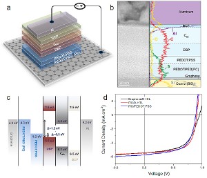
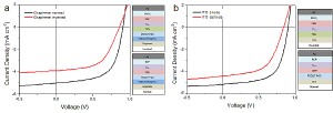
The high transparency of graphene[1], together with its good electrical conductivity[2] and mechanical robustness[3], enable its use as transparent electrodes in optoelectronic devices such as solar cells. While initial demonstrations of graphene-based organic photovoltaics (OPV) have been promising, realization of scalable technologies remains challenging due to their performance and, critically, their poor device reproducibility and yield. In this work, by engineering the interface between graphene and organic layers, we demonstrate that device performance and yield become close to that of devices using indium tin oxide. Our study confirms that the key issue leading to the poor performance or irreproducibility in graphene-based OPV originates from the graphene interface and can be addressed by a simple interface modification method introduced in this work. This interface modification is achieved by inserting a thin polymeric buffer layer between the pristine graphene surface and the PEDOT:PSS hole injection layer (HIL), thus forming a double-HIL structure (D-HIL) (Figure 1). We also demonstrate that this method can be further expanded to the inverted solar cell geometry, using TiOx or ZnO as the electron-transporting and hole-blocking layer, where graphene is utilized as the cathode, thus illustrating the broad application of graphene as a transparent conductor in OPV in general (Figure 2). By engineering the interfacial HIL between the graphene electrode and the organic donor layer, we find that the performance and yield of graphene-based OPV devices become close to those of devices using ITO electrodes. This work takes one step forward in the realization of graphene as a viable replacement for or alternative to ITO for various optoelectronic device applications.
- Figure 1: Composition and device performance of typical organic solar cells using graphene anodes. (a) Schematic diagram of the graphene anode OPV architecture: graphene/PEDOT:PEG(PC), 40nm/PEDOT:PSS, 20nm/DBP, 25nm/C60, 40nm/BCP, 8.5nm/Al, 100nm. (b) Cross-sectional TEM image (left) of the complete device described in (a), with an energy dispersive EDS elemental line scan overlaid on a schematic of the device cross-section (right). (c) Flat-band energy level diagram of the completed OPV device. (d) Current density vs. voltage (J-V) characteristics of a representative graphene device (using D-HIL, black) compared with ITO reference cells (red and blue) under simulated AM 1.5G illumination at 100 mW∙cm-2, illustrating comparable performances.
- Figure 2: J-V characteristics of inverted small molecule solar cells with TiOx ESL. (a) On D-HIL modified graphene and (b) on ITO under AM 1.5G at 100 mW∙cm-2. Device performances with normal geometry are shown for comparison. J-V characteristics of representative graphene and ITO devices with ZnO ESL. Using (c) small molecule photoactive layers and (d) P3HT:PCBM photoactive layer under AM 1.5G at 100 mW∙cm-2.
- R. Nair, P. Blake, A. Grigorenko, K. Novoselov, T. Booth, T. Stauber, N. Peres, and A. Geim “Fine structure constant defines visual transparency of graphene,” Science, vol. 320, no. 5881, pp. 1308-1308, 2008. [↩]
- K. Bolotin, K. Sikes, Z. Jiang, M. Klima, G. Fudenberg, J. Hone, P. Kim, and H. Stormer, “Ultrahigh electron mobility in suspended graphene,” Solid State Commun., vol. 146, no. 9-10, pp. 351-355, 2008. [↩]
- J. Bunch, A. van der Zande, S. Verbridge, I. Frank, D. Tanenbaum, J. Parpia, H. Craighead, and P. McEuen, “Electromechanical resonators from graphene sheets,” Science, vol. 315, no. 5811, pp. 490-493, 2007. [↩]

