Contact-printed MEMS Membranes
- Category: MEMS & BioMEMS
- Tags: apoorva murarka, vladimir bulovic
It is desirable to extend the functionality of MEMS to different form factors including large-area arrays of sensors and actuators, and to various substrate materials, by developing a means to fabricate large-area suspended thin films. Conventional photolithography-based MEMS fabrication methods limit the device array size and are incompatible with flexible polymeric substrates[1][2].
A new method for additive fabrication of thin (125±15-nm-thick) gold membranes on cavity-patterned silicon dioxide substrates using contact-transfer printing is presented for MEMS applications. The deflection of these membranes, suspended over cavities in a silicon dioxide dielectric layer atop a conducting electrode, can be used to produce sounds or monitor pressure. The fabrication process employs a novel technique of dissolving an underlying organic film using acetone to transfer membranes onto the substrates. The process avoids fabrication of MEMS diaphragms via wet or deep reactive-ion etching, which in turn removes the need for etch-stops and wafer bonding. Membranes up to 0.78 mm2 in area are fabricated, and their deflection is measured using optical interferometry. The membranes have a maximum deflection of about 150 nm across 28-μm-diameter cavities, as shown in Figure 1[3]. Using the membrane deflection data, Young’s modulus of these gold films is extracted (74±17 GPa), and it is comparable to that of bulk gold. Additionally, a 15 Hz sinusoidally varying voltage of 15 V peak-to-peak amplitude is applied to the MEMS device to demonstrate that the large membrane deflection is a repeatable deflection (Figure 2).
These films can be utilized in microspeakers, pressure sensors, microphones, deformable mirrors, tunable optical cavities, and large-area arrays of these devices.
-

- Figure 1: Deflection profiles of gold membranes under electrostatic actuation, obtained via optical interferometry. (a) Deflection of the membrane increases as the voltage applied between the membrane and the Si substrate increases. (b) 13 different diametrical deflection profiles (inset: interferometry image) of a membrane under 15 V actuation are plotted and averaged to show the mean profile. (c) Gold membrane deflection over multiple cavities covered by a single membrane, as the voltage is increased from 1 V to 15 V.
-
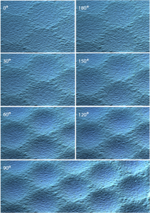
- Figure 2: Optical interferometry images of several cavities under 15 V peak-to-peak amplitude sinusoidal voltage actuation at 15 Hz, taken at 30 degree phase intervals. Membrane deflection for only one half of a sine wave is shown in this figure.
- A. Murarka, C. Packard, F. Yaul, J. Lang, and V. Bulovic, “Micro-contact printed MEMS,” IEEE 24th International Conference on Micro Electro Mechanical Systems (MEMS), 2011, pp. 292-295. [↩]
- C. Packard, A. Murarka, E. W. Lam, M. A. Schmidt, and V. Bulovic, “Contact-printed microelectromechanical systems,” Advanced Materials, vol. 22, pp. 1840–1844, 2010. [↩]
- A. Murarka, S. Paydavosi, T. L. Andrew, A. I. Wang, J. H. Lang, and V. Bulovic, “Printed MEMS membranes on silicon,” IEEE 25th International Conference on Micro Electro Mechanical Systems (MEMS), 2012, pp. 309-312. [↩]