- Authors: M. S. Dresselhaus, P. T. Araujo
- Sponsorship: NSF
Paulo T. Araujo has been using MTL facilities through 2011/2012 to fulfill one step of his device fabrication. In general, the devices are made by graphite exfoliation so that a single layer of graphene is sitting on a 300-nm-thick layer of SiO2. After the standard lithography steps used to design from two to four contacts over the graphene layer, titanium and gold are deposited. The metals are deposited by utilizing the e-beam evaporator from EML at MTL headquarters. The devices were used in gate-modulated Raman experiments, which allow us to observe phonon energy renormalizations by observing gate-voltage dependent changes in its Raman signatures [] [] [] [] .
- Authors: K. K. Kim, A. Hsu, X. Jia, S. M. Kim, Y. Shi, M. Hofmann, D. Nezich, J. F. Rodriguez-Nieva, M. Dresselhaus, T. Palacios, J. Kong
- Sponsorship: NSF, ONR GATE-MURI
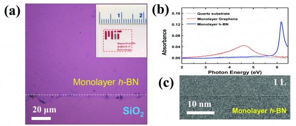
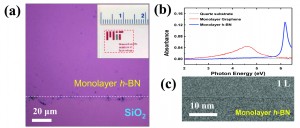
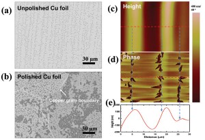
Hexagonal boron nitride (h-BN) is very attractive for many applications, particularly as a protective coating, dielectric layer/substrate, transparent membrane, or deep ultraviolet emitter. In this work, we carried out a detailed investigation of h-BN synthesis on Cu substrate using chemical vapor deposition (CVD) with two heating zones under low pressure (LP). Previous atmospheric pressure (AP) CVD syntheses were able to obtain only a few layers of h-BN without a good control on the number of layers [] [] . In contrast, under LPCVD growth, monolayer h-BN was synthesized, and time-dependent growth was investigated (Figure 1). It was also observed that the morphology of the Cu surface affects the location and density of the h-BN nucleation (Figure 2). Ammonia borane, which is easily accessible and more stable under ambient conditions than borazine, is used as a BN precursor. The h-BN films are characterized by atomic force microscopy, transmission electron microscopy and electron energy loss spectroscopy analyses. Our results suggest that the growth here occurs via surface-mediated growth, which is similar to graphene growth on Cu under LP. These atomically thin layers are particularly attractive for use as atomic membranes or dielectric layers/substrates for graphene devices [] .
-
-
Figure 1: Monolayer h-BN characterization. (a) Optical image of h-BN on 300 nm SiO2/Si. White dotted line indicates the border between h-BN and SiO2. The inset displays a photograph of h-BN film on a quartz substrate (red dotted area). (b) Optical absorption spectra of a monolayer h-BN, monolayer graphene and a quartz substrate (as a reference). (c) TEM image of the folded edge of a monolayer h-BN.
-
-
Figure 2: Effect of copper surface morphology on h-BN growth. SEM images of (a) an unpolished copper foil and (b) a polished copper foil after h-BN growth for 10 min with T1=70 oC. (c)-(d) AFM images of the unpolished copper foil after growth: (c) height and (d) phase images. (e) Height profile along the red dotted in (c) and (d).
- Authors: X. Zhang, K. K. Kim, J. Kong, M. Dresselhaus, T. Palacios
Graphene, a two-dimensional honeycomb lattice of sp2-hybridized carbon atoms, has attracted tremendous interest in the scientific community. Surface functionalization is a technology to engineer its electronic properties and make it even more desirable and controllable for electronic device applications. For example, chemical functionalization of graphene, especially by hydrogen, fluorine, and chlorine is predicted to enable doping, edge passivation, and opening of its bandgap. Here, we demonstrate that exposure of graphene device to chlorine plasma in an electron cyclotron resonance (ECR) plasma etcher is an effective way to tune the Fermi level of graphene carriers towards p-type direction, without sacrificing its high conductivity.
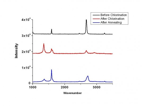
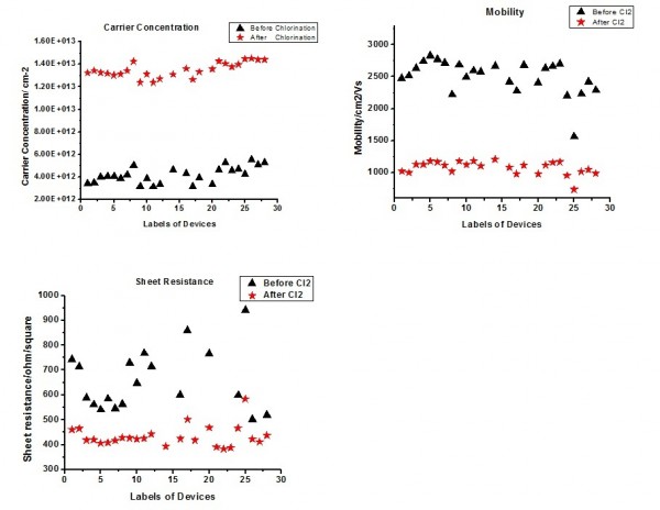
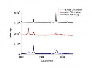
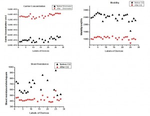
Figure 1 compares the Raman spectroscopy of graphene before and after chlorine plasma treatment and also shows how it changes after annealing. After chlorine plasma treatment for 30 s, the D band increases substantially while the G band blue shift by about 5 cm-1. More importantly, the D band decreases significantly after a 30-min annealing at 500 °C, which means little defect creation occurs during the plasma process. Further transport measurement shows that the carrier concentration in graphene increases considerably. The plasma reaction process tunes the Fermi level of an intrinsic p-type CVD graphene (VDirac >0) towards p-type direction further. We notice that the carrier mobility reduces after plasma reaction. However, this reduction should be mainly due to the increase of hole concentration in graphene rather than defect creation, which is confirmed by the decrease of its sheet resistance and increase of conductivity (see Figure 2). In addition, XPS analysis shows that the percentage of chlorine on the surface of graphene is around 20%. This approach indicates an important way to engineer graphene properties for high-performance applications of graphene devices.
-
-
Figure 1: Raman spectroscopy of graphene before plasma treatment, after plasma treatment, and after annealing.
-
-
FIgure 2: Comparison: conductivity, carrier concentration, mobility and sheet resistance of graphene devices before and after chlorination.