Duane S. Boning
Collaborators
- Y.-C. Lam, NTU, Singapore
- A. Philipossian, Univ. of Arizona
Graduate Students
- K. Balakrishnan, Res. Asst., EECS
- A. Chang, Res. Asst., EECS
- W. Fan, Res. Asst., EECS
- C. GoGwilt, Res. Asst., EECS
- J. Lee, Res. Asst., EECS
- J. Johnson, Res. Asst., EECS
- L. Yu, Res. Asst., EECS
Support Staff
- M. Whiting, Admin. Asst. II
Publications
W. Fan, D. Boning, L. Charns, H. Miyauchi, H. Tano, and S. Tsuji, “Study on Stiffness and Conditioning Effects of CMP Pad Based on Physical Die-level CMP Model,” J. Electrochem. Soc., vol. 157, no. 5, pp. H526-H533, May 2010.
H. Taylor, M. Hale, Y. C. Lam, and D. Boning, “A method for the accelerated simulation of micro-embossed topographies in thermoplastic polymers,” J. Micromechanics and Microengineering, vol. 20, no. 6, p. 065001, June 2010.
H. Taylor, Y. C. Lam, and D. Boning, “An investigation of the detrimental impact of trapped air in thermoplastic micro-embossing,” J. Micromechanics and Microengineering, vol. 20, no. 6, p. 065014, June 2010.
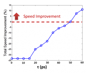
N. Drego, A. Chandrakasan, D. Boning, and D. Shah, “Reduction of Variation-Induced Energy Overhead in Multi-core Processors,” IEEE Trans. on Computer-Aided Design, vol. 30, no. 6, pp. 891-904, June 2011.
H. Taylor, K. Smistrup, and D. Boning, “Modeling and simulation of stamp deflections in nanoimprint lithography: exploiting backside grooves to enhance residual layer thickness uniformity,” Microelectronic Engineering, vol. 88, no. 8, pp. 2154-2157, August 2011.
H. Taylor, D. Boning, and C. Iliescu, “A razor-blade test of the demolding energy in a thermoplastic embossing process,” Journal of Micromechanics and Microengineering, vol. 21, no. 6, p. 067002, June 2011.
R. K. Jena, H. K. Taylor, Y. C. Lam, D. S. Boning, and C. Y. Yue, “Effect of polymer orientation on pattern replication in a micro-hot embossing process: experiments and numerical simulation,” Journal of Micromechanics and Microengineering, vol. 21, no. 6, p. 065007, June 2011.
H. Taylor, K. Smistrup, and D. Boning, “Modeling and simulation of stamp deflections in nanoimprint lithography: exploiting backside grooves to enhance residual layer thickness uniformity,” 36th International Conference on Micro & Nano Engineering (MNE2010), Genoa, Sept. 2010.
W. Fan, J. Johnson, and D. S. Boning, “Non-Ohmic Wafer-Level Modeling of Electrochemical-Mechanical Planarization (ECMP),” International Conference on Planarization Technology (ICPT), Phoenix, AZ, Oct. 2010.
D. Boning, A. Kahng, H. Taylor, and Y.-K. Wu, “Chip-Scale Simulation of Residual Layer Thickness Uniformity in Thermal Nanoimprint Lithography: Evaluating Stamp Cavity-Height and ‘Dummy-Fill’ Selection Strategies,” 9th International Conference on Nanoimprint and Nanoprint Technology (NNT), Copenhagen, Denmark, Oct. 2010.
H. Taylor, K. Simstrup, and D. Boning, “Modeling the Enhancement of Nanoimprint Stamp Bending Compliance by Backside Grooves: Mitigating the Impact of Wafer Nanotopography on Residual Layer Thickness,” 9th International Conference on Nanoimprint and Nanoprint Technology (NNT), Copenhagen, Denmark, Oct. 2010.
J. O. Diaz, H. K. Taylor, R. J. Shul, R. L. Jarecki, T. M. Bauer, D. S. Boning, and D. L. Hetherington, “A Computationally Simple, Wafer-to-Feature-Level Model of Etch Rate Variation in Deep Reactive Ion Etching,” AVS 57th International Symposium & Exhibition, Albuquerque, NM, Oct. 2010.
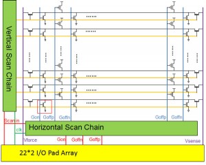
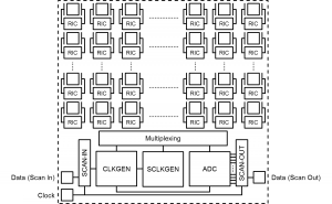
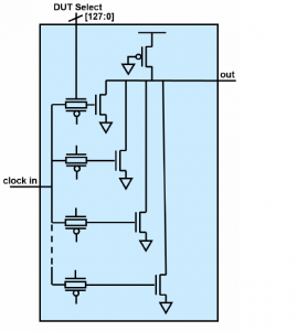
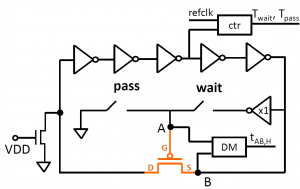
K. Balakrishnan, K. Jenkins, and D. Boning, “A Simple Array-Based Test Structure for the AC Variability Characterization of MOSFETs,” IEEE International Symposium on Quality Electronic Design (ISQED), March 2011.
A. H. Chang, D. Boning, and H.-S. Lee, “Redundancy in SAR ADCs,” Great Lakes Symposium on Very Large Scale Integration (GLSVLSI), Lausanne, Switzerland, May 2011.
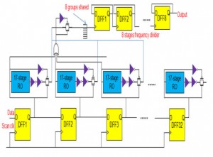
K. Balakrishnan, K. A. Jenkins, and D. Boning, “A Ring Oscillator-Based Test Structure for AC Variability Characterization of Individual MOSFETs,” 2nd European Workshop on CMOS Variability (VARI), 4 pages, Grenoble, France, May 2011.
Fan, W., J. Johnson, and D. Boning, “Wafer-level Modeling of Electrochemical-Mechanical Planarization (ECMP),” International Conference on Planarization Technology (ICPT), Phoenix, AZ, Oct. 2010.
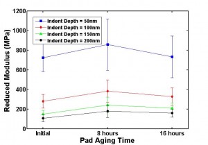
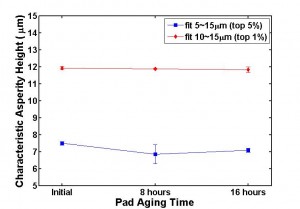
W. Fan, D. Boning, Y. Zhuang, Y. Sampurno, A. Philipossian, D. Hooper, and M. Moinpour, “Characterization of CMP Pad Surface Properties,” Clarkson Workshop on Chemical-Mechanical Polishing, Lake Placid, NY, Aug. 2010.
D. Boning, A. H. Chang, K. Zuo, J. Wang, and D. Yu, “Test Structures, Circuits, and Extractions Methods for Determining Pattern Density Effects,” IEEE/ACM Workshop on Variability Modeling and Characterization (VMC), San Jose, CA, Nov. 11, 2010.
