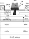
InGaSb p-channel Quantum-Well MOSFETs and FinFETs
As concerns grow over the feasibility of scaling silicon CMOS devices to the nanometer regime, III-V channels have shown great promise for integration into future-generation logic devices due to their outstanding electron transport properties. However, while impressive III-V n-MOSFETs have been demonstrated, this success has not yet been translated to III-V p-MOSFETs, due to a generally lower hole mobility. Amongst all III-V materials, the antimonide system has the highest hole mobility, making it a likely candidate for the development of high performance III-V p-MOSFETs. At MIT, we are exploring the suitability of InGaSb for p-channel MOSFETs for future sub-10 nm CMOS applications.
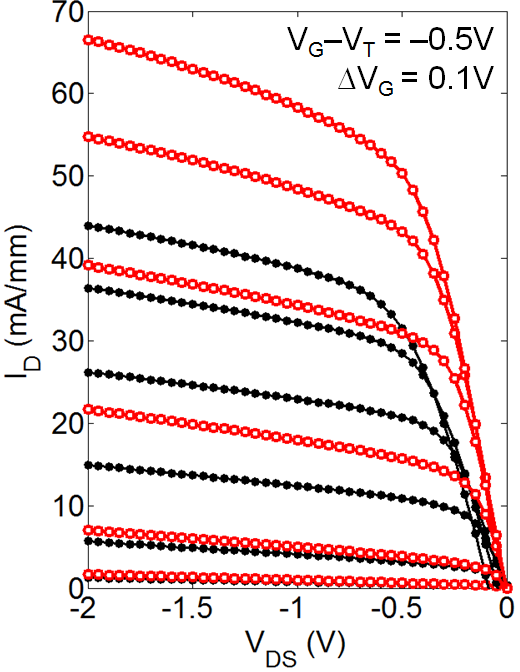
Our research has focused on device designs that incorporate strong compressive strain which is known to enhance hole mobility. In this regard, we have demonstrated InGaSb p-channel quantum-well (QW) MOSFETs that incorporate uniaxial stress through a self-aligned nitride stressor. We have realized improvements in transconductance that exceed 40% with respect to strain-free devices. In addition, we have developed a new approach to ohmic contacts to InGaSb FET structures that has yielded large improvements in contact resistance and in the transport characteristics of completed devices.
Recent publications:
RJ-158 Guo, L. W., W. Lu, B. R. Bennett, J. B. Boos, and J. A. del Alamo, Ultra-low Resistance Ohmic Contacts for p-channel InGaSb Field-Effect Transistors. IEEE Electron Device Letters, Vol. 36, No. 6, pp. 546-548, June 2015. (paper)
RJ-150 Guo, L. W., L. Xia, B. R. Bennett, J. B. Boos, M. G. Ancona and J. A. del Alamo, Enhancing p-channel InGaSb QW-FETs via Process-induced Compressive Uniaxial Strain. IEEE Electron Device Letters, Vol. 35, No. 11, pp. 1088-1090, November 2014. (paper)
RJ-129 Xia, L., B. Boos, B. R. Bennett, M. G. Ancona, and J. A. del Alamo, "Hole Mobility Enhancement through <110> Uniaxial Strain in In0.41Ga0.59Sb Quantum-Well Field-Effect transistors." Applied Physics Letters, Vol. 98, 053505, 2011. (paper)
|
|