Validation of an Ultra-compact Virtual Source FET Model for Deeply Scaled Standard Cell Libraries and Digital Circuits
- Category: Circuits & Systems
- Tags: duane boning, li yu
In this work, the virtual source (VS) charge-based compact model is validated for standard cell libraries and digital circuits. The VS model is a simple analytical ultra-compact model for deeply scaled CMOS transistors with guaranteed continuity in current, charges, and their derivatives in all operation regions [1] [2] . With only a modest number of physically meaningful parameters, the extended VS compact model includes all of the main physical effects in nanometer technologies. The VS model is verified with simulated data from a well-characterized, industrial 40-nm bulk silicon model. Standard cell library characterization is also conducted using both the VS FET model and its “golden” industrial counterpart with excellent agreement between the timing results of the two models. Finally, a 1001-stage inverter chain and a 32-bit ripple-adder are employed as test cases in a vendor CAD environment to validate the use of the VS model for large-scale digital circuit applications. Parametric Vdd sweeps show that the VS model is ready for usage in low-power design methodologies.
The first circuit we consider is an inverter undergoing trapezoidal input transitions. This basic example is used to illustrate several important features of our calibrated VS model. It is well known that the charging and discharging activities during input gate transitions require precise balancing of both static and dynamic behavior of the NFET and PFET transistors. The output voltage waveforms using the VS model in comparison with the industry-standard BSIM4 model are depicted in Figure 1. The input slew is fixed at 10ps and the load (fanout) are 1, 2, and 4. The average delay error between the VS model and the “golden” or baseline BSIM4 model is 0.88%, and the 10% -90% rising/falling time errors are 0.92%/1.11%. This timing error is a good indication of the accuracy of the transient calibration of the proposed VS model.
To further verify the calibrated VS model, a 32-bit ripple-carry adder is designed in the targeted technology (40-nm bulk CMOS), and the transient waveform of the critical path is compared using VS and BSIM4 models. The simulation environment and the SPICE convergence setting using both models are exactly the same. The test circuit includes 0.9k transistors in total belonging to various library cell types (INV, NAND, NOR and XOR). We select the worst-case delay for a 32-bit add operation. To show the robustness of the VS model for low-power design, the supply voltage Vdd is swept from 0.6V to 0.9V. The transient signals Cin0 and Cout32 at different Vdd from both VS and BSIM4 model are shown in Figure 2, which demonstrates that the output signals of the two models have excellent matching. The average delay mismatch under all Vdd conditions is about 0.3%. The simulation we conduct achieves an average runtime speed up of 7.6X, which is in line with the order of magnitude reduction in the number of VS parameters.
-
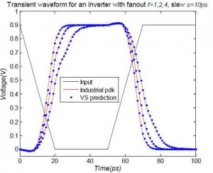
- Figure 1: Transient response waveform for an inverter chain with various input fanouts.
-
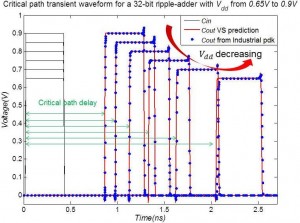
- Figure 2: Critical path transient waveform for a 32-bit ripple-adder with Vdd from 0.65V to 0.9V.
- A. Khakifirooz et al. “A simple semi-empirical short-channel MOSFET current-voltage model continuous across all regions of operation and employing only physical parameters,” IEEE Trans. on Electron Devices, pp. 1674-1680, Aug. 2009. [↩]
- L. Wei et al. “Virtual-source-based self-consistent current and charge FET models: From ballistic to drift-diffusion velocity-saturation operation,” IEEE Trans. on Electron Devices, pp. 1-9, 2012. [↩]