- Authors: Z. Mahmood, R. Suaya, L. Daniel
- Sponsorship: SRC/FCRP IFC, Mentor Graphics
Automatic generation of accurate, compact, and passive dynamical models for multiport linear structures such as interconnects is a crucial part of the overall design procedure for complex circuits. First, frequency response samples for multiport linear structures are collected from either an electromagnetic field solver or physical measurements. Second, a compact model is developed that can be incorporated into a circuit simulator for time-domain simulations of a larger system also containing nonlinear devices. For these compact models, even a small violation of any basic property of the structure, such as passivity, can cause large errors in the response of the overall system, and the results can become completely nonphysical. It is, therefore, essential to preserve basic system properties during the model identification. To model multiport structures from given frequency response samples, the approaches based on convex optimization [] are very expensive and quickly exhaust available computational resources such as memory. These approaches can be used to model only structures having a much smaller number of ports. Other techniques identify a stable, but non-passive, model, and then perturb the model to make it passive [] . However, such approaches suffer from limitations if the initial non-passive model has significant passivity violations.
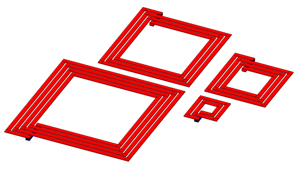
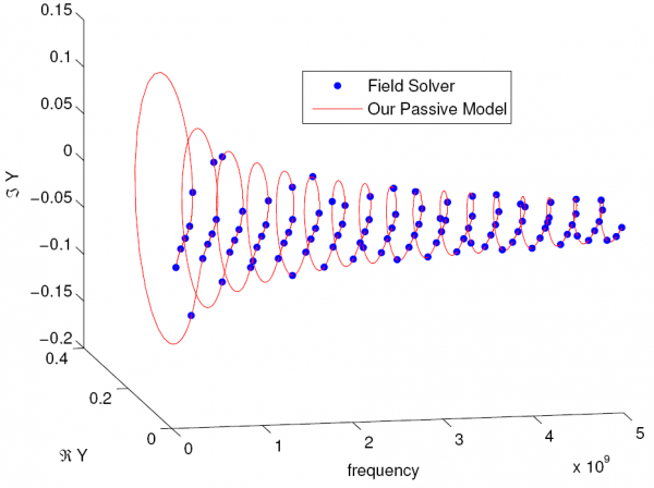
In this work, we are developing an efficient modeling framework that will automatically generate accurate, compact, and passive dynamical models for multiport linear systems. Given measured transfer function samples, we identify a rational transfer function model that minimizes the mismatch at the given frequencies. These dynamical models can be interfaced with commercial circuit simulators for time-domain simulations of a larger interconnected system. To guarantee the stability of the overall simulation, we ensure the passivity of our generated models by enforcing semidefinite constraints during the fitting process as proposed in [] [] . Figure 1 shows the layout of coupled RF inductors, which is one of the structures we used for testing our algorithm. Figure 2 compares the output of our identified model with the given data for a four-port structure. Furthermore, for the same model order, we get orders-of-magnitude improvement in terms of both speed and memory compared to [] .
-

-
Figure 1: Layout of coupled RF inductors.
-

-
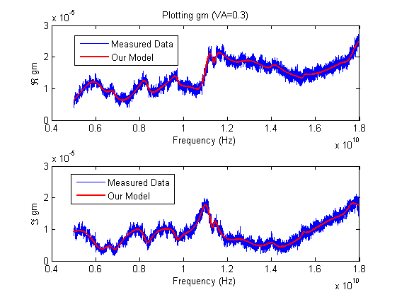
Figure 2: [4-port structure] Blue dots indicate the given Y11 frequency response samples. The red solid line is the Y11 from our identified model.
- Authors: A. Hochman, J. Villena, Z. Mahmood, L. Wald, E. Adalsteinsson, J. White, L. Daniel
- Sponsorship: NIH, MIT-SkTech
Two recent advances in Magnetic Resonance Imaging (MRI) technology have resulted in a need for sophisticated computational electromagnetics (CEM) tools. The first is the availability of higher fields scans that can improve signal-to-noise ratio. The second is the availability of transmit-coil arrays, which can be used to minimize human-body heating by electric fields. Higher fields imply higher-frequency RF pulses, with wavelengths comparable to the human body dimensions, which complicates electromagnetic analysis. They also imply increased tissue heating, which limits the RF power used for imaging purposes. In the computational prototyping group, we are developing CEM techniques to address these new needs of the MRI community, working in close collaboration with the RLE MRI group and the Harvard Massachusetts General Hospital MRI group, with some specific targets.
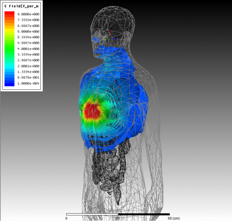
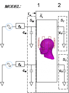
First, we are developing fast methods for tuning and matching the transmitters to the human-body loaded MRI coils. We combined scattering-matrix formalism, a frequency-domain finite-elements method, and commercial RF optimization software to reduce this process from days to hours. Also we plan to apply integral-equation methods to reduce it to minutes. Second, we are developing integral methods to allow for efficiently optimizing the geometrical configuration of the transmit coils. This hybrid approach will combine pre-computed Green’s functions for a realistic human body model with method of moments to be able to rapidly assess different coil configurations for a typical body. To aid this assessment, we plan to leverage our work on parameterized model-order reduction, automatically generating models depending on relevant parametric quantities. We are also working on fast methods for computing the approximate solutions to the electromagnetic fields inside the human body, assuming a simplified 3-tissue model that can be obtained for each patient by a quick MRI scan. Finally, we are developing an automated procedure for designing robust decoupling networks for arbitrary MRI transmission coil arrays, based on automatic nonlinear least squares techniques to compute the input impedance matrix, in opposition to currently applied manual methods, limited to small number of channels. These decoupling networks reduce the input power required for the same local increase of body heat vs. excitation fidelity.
-
-
Figure 1: A scattering matrix formalism is used to generate a model for the transmit coils loaded by a human head. This model is then used in a commercial RF optimization package (RF Designer) to tune and match the coils to their drivers.
-

-
Figure 2: Electric fields generated by a 10A current source about 5 cm away from the chest, obtained by the commercial HFSS package. Similar calculations are performed for such sources at points around the body. These fields yield a numerically calculated Green’s function for the human body, which can then be used in an integral-equation method to rapidly assess different coil configurations.
- Authors: Z. Mahmood, R. Marathe, D. Weinstein, L. Daniel
- Sponsorship: SRC/FCRP IFC, NSF, SRC/FCRP IFC, NSF
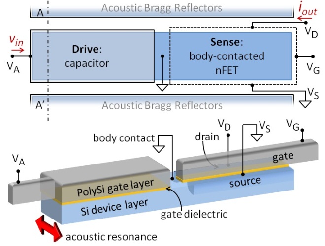
Design and optimization of novel RF Nano-Electro-Mechanical (NEM) resonators such as Resonant Body Transistors (RBT) require modeling across multiple domains, including mechanical (distributed stress and elastic wave models), electrical (semiconductor devices and RF small signal models), and thermal. These domains are all cross-coupled in nonlinear ways and require lengthy finite element multi-physics analyses to solve. Due to the complexity of these structures embedded in the CMOS stack and sensed using active FETs, the day-long time scale of each finite element simulation prevents quick, intuitive parameterization of device design. A reduced model parameterized across all three domains is therefore necessary both for rapid prototyping and for device optimization.
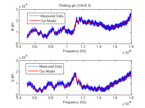
In this work, we are developing an algorithm to automatically generate compact models for NEM resonators. Our compact models are suitable for AC, DC and RF operation of the device and allow the circuit designers to run circuit-level time-domain simulations using any commercial circuit simulator [] [] . The compact models are “parameterized,” so that the circuit designer will be able to instantiate instantaneously models within the circuit simulator for different values of the key device parameters. Key resonator parameters included in the compact parameterized model are resonant frequency, quality factor, signal strength, isolation, presence of spurious modes, and operating temperature. Values for the model coefficients are calibrated using measurements from NEMS resonator devices. A critically important feature of our models is to guarantee that when circuit designers change arbitrarily values for the device parameters, the compact models will always preserve the physical properties of the original device and will never cause numerical instabilities and convergence issues when connected to other device models and circuits within the circuit simulator [] . Figure 1 shows the layout of a Si-based NEMS-CMOS resonator. Numerical results show a great promise for our technique. We have achieved high quality fit to the measured data, as Figure 2 shows, which offered modeling challenges including the presence of noise and spurious resonant peaks.
-
-
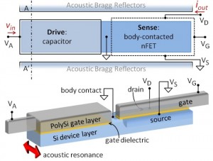
Figure 1: Top and 3D views of a Si-based NEMS-CMOS.
-
-
Figure 2: Plotting measured data (blue noisy line) and the output from out model (red smooth line) for controlling voltage VA=0.3V.