Simulation of Two-dimensional Core-shell Structures for Broadband Solar Cell Absorption
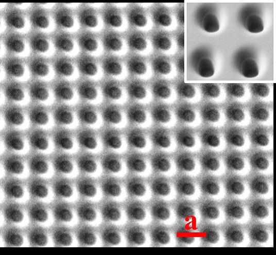
Solar cells with broadband absorption and large acceptance angle are demonstrated by using two-dimensional core-shell structures, which are composed of silicon oxide shells and silicon cores. This study considers structure parameters such as core/shell thickness and periodicity. Finite difference time domain calculation (FDTD) is used in the simulation. As Figure 1 shows, our core-shell structure is built of Si and SiOx with a feature size much smaller than the wavelength of light. The core can be either amorphous or polycrystalline silicon, and the shell is silicon dioxide. Four structural parameters are considered: outer radius (r1), inner radius (r2), height (h), and periodicity (a) or symmetry. By tuning these four parameters, we are able to generate an antireflection effect that covers the entire silicon absorption spectrum.
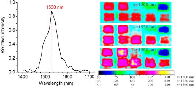
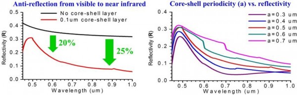
Figure 2 (a) highlights the superior antireflective property of the core-shell layer from our study. An enhancement of absorption is observed between wavelengths of 400-1200 nm. Strong antireflection is achieved as a 0.1-um-thick core-shell layer is applied. The reflectivity drops significantly by 20% at wavelength λ=600 nm and 25% at λ=900 nm. Figure 2 (b) shows that the reflectivity reduces as the periodicities decrease. A huge drop of 20% in reflectivity is observed at wavelength of 0.7 um as the periodicities change from 0.7 um to 0.3 um. The reflectivity within this range is uniformly low. We note that the broadband absorption spectra are not sensitive to the light incident angles. The large acceptant angle is contributed by the continuous varied refractive indexes. Hence, by using the core-shell structure, we improve the efficiency of solar cells by minimizing the loss caused by surface reflection. The easy fabrication of the core-shell structure enables large-scale fabrication of highly efficient solar cells.
-
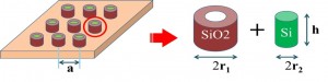
- Figure 1: The layouts and the composition of core shell structures. The core-shell structures can be analyzed by the parameters: outer radius (r1), inner radius (r2), height (h), and periodicity (a).

-
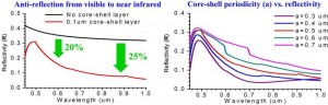
- Figure 2: (a) The reflection spectra of silicon thin films with and without a 0.1-µm-thick core-shell structures. (b) The reflection spectra of core-shell structures with periodicities of 0.3 µm, 0.4 µm, 0.5 µm, 0.6 µm and 0.7 µm, respectively.
- P. T. Lin, Y. Yi, X. Duan, and L. C. Kimerling, “Simulation and fabrication of two-dimensional core-shell structures for broadband solar cells absorption,” presented at MRS Fall Meeting & Exhibit, Boston, J7.20, 2011.