Ultra-Fast Pulsed High-Current Cold Cathodes with Temporal and Spatial Emission Uniformity
Field emission arrays (FEAs) are an attractive alternative to mainstream thermionic cathodes, which are power hungry and require high vacuum and high temperature to operate. Field emission of electrons consists of the following two processes: 1) transmission of electrons (tunneling) through the potential barrier that holds electrons within the material (workfunction φ) when the barrier is deformed by the application of a high electrostatic field and 2) supply of electrons from the bulk of the material to the emitting surface. Either the transmission process or the supply process could be the limiting step that determines the emission current of the field emitter (FE). Control of the transmission process (Fowler Nordheim) to produce high uniform current from FEAs is very challenging due to the physics of the field emission process. Due to the exponential dependence on the field factor and, hence, the tip radius, emission currents are extremely sensitive to tip radii variation; unfortunately, nanometer-sized tip radii in FEAs have a distribution with long tails that causes severe FEA underutilization. A better approach for achieving uniform emission from nanosharp FEAs is controlling the supply of electrons to the emitting surface. In a metal, the supply of electrons is very high, making the control of the supply challenging. However, in a semiconductor, where the local doping level and the local potential determine the concentration of electrons, it is possible to configure the emitter such that either the supply process determines the emission current.
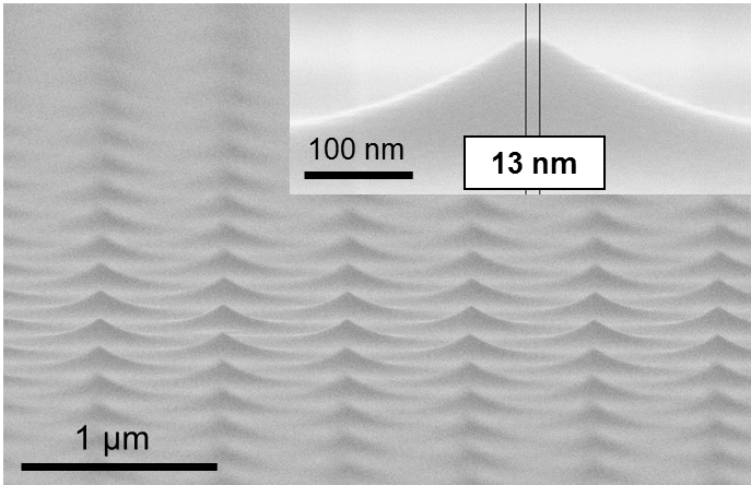
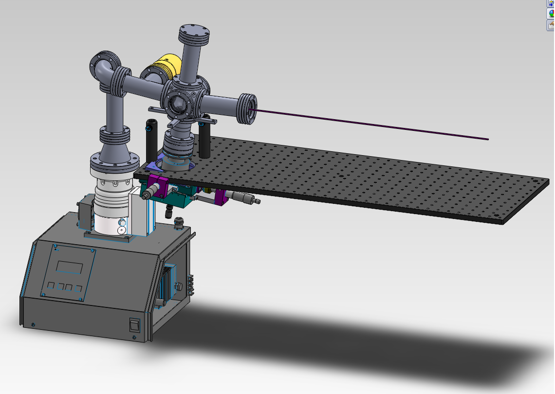
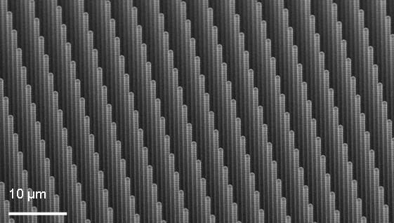
We have designed and fabricated FEAs where each field emitter is individually ballasted using a vertical ungated field effect transistor (FET) made from a high aspect ratio (40:1) n-type silicon pillar. Each emitter has a proximal extractor gate that is self-aligned for maximum electron transmission to the anode (collector). Our modeling suggests that these cathodes can emit as much as 30 A.cm-2 uniformly with no degradation of the emitters due to Joule heating; also, these cathodes can be switched at microsecond-level speeds. The design process flow, mask set and pillar arrays have been completed (Figure 1) with the self-aligned extractor gate to be completed by the spring of 2013. An ultra-high vacuum chamber has been designed and built to test the devices (Figure 2). The chamber can test full 150mm wafers with four high voltage probes at 10-10 torr pressure.
-
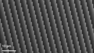
- Figure 1: Large array of high aspect ratio pillars with 10nm radius tips with 5 µm hexagonal packing for individually ballasted field emission arrays.
-
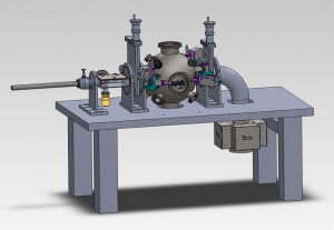
- Figure 2: CAD drawing of the UHV chamber design that is capable of testing 150 mm wafer with four high voltage probes at 10-10 torr.