- Authors: F. A. Hill, L. F. Velásquez-García
- Sponsorship: DARPA
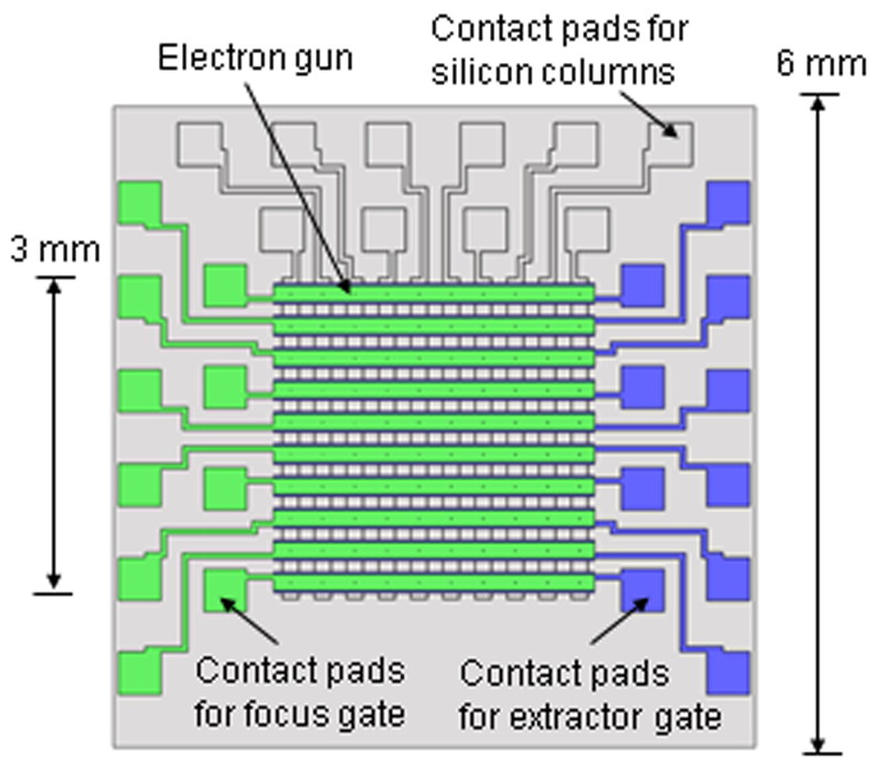
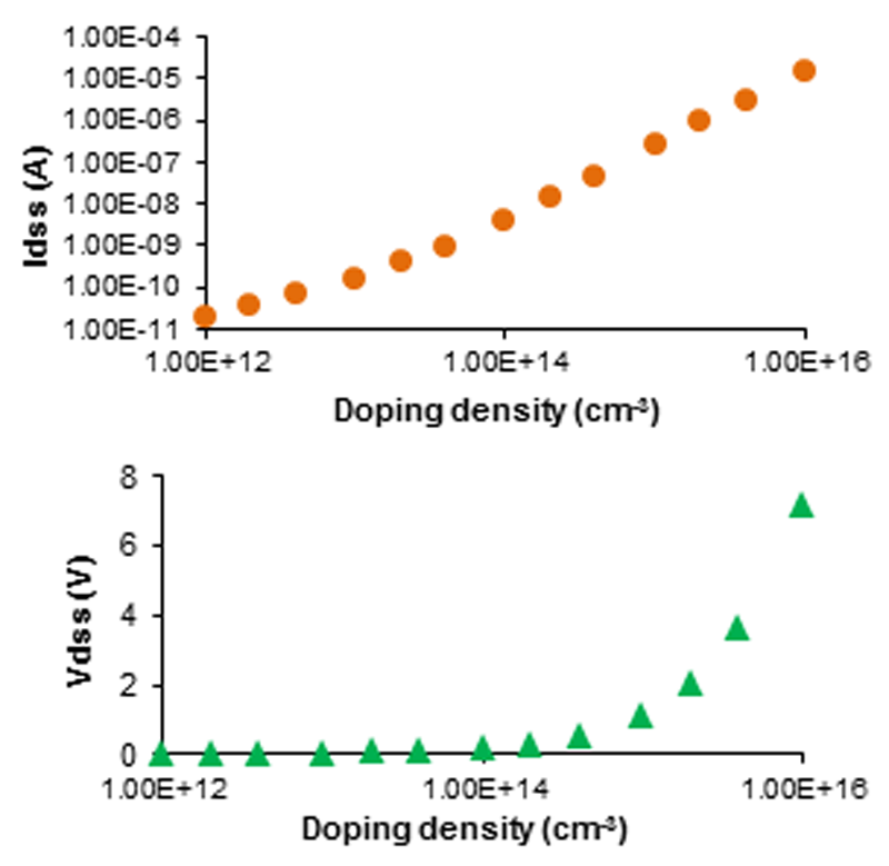
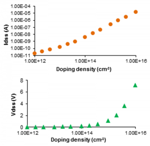
This work focuses on the design and fabrication of a cathode for a portable x-ray source. The cathode is made of an array of individually addressable electron guns, each containing double-gated field emitters. Compared to thermionic cathodes, field emission arrays operate at lower vacuum and lower temperatures, use less power and are more portable. The electron beam from each gun is extracted by a proximal gate and collimated using a distal gate before it hits an anode in a micron-sized spot that generates Bremsstrahlung x-rays. The architecture of the cathode is shown in Figure 1. Each field emitter is fabricated on top of a vertical ungated field-effect transistor (FET) [] [] that acts as a current source due to the velocity saturation of electrons in silicon when the voltage across the FET is above a saturation voltage. Current source-like behavior provides spatial and temporal uniformity of the output current across the emitter array; it also protects against emitter burnout and current surges. Individual addressability is achieved by fabricating the structure on SOI wafers to create electrically isolate strips of silicon. The extractor and focus gates are monolithically integrated with the cathode chip. They are patterned in strips that are orthogonal to the silicon strips, so that a single electron gun can be turned on at once. Each vertical ungated FET is a 25-μm-tall column with a 0.5-μm diameter, and emitter tip radius is in the range of 20 nm. The saturation current and saturation voltage of the silicon columns are plotted as a function of doping density in Figure 2. Wafer doping of 10-20 Ω cm provides a saturation current of 0.5 μA and an output impedance of 2×10⁹ Ω. With 100 emitters per chip, the total output current per chip is 50 μA, corresponding to a current density of 139 μA/cm2.
-

-
Figure 1: Architecture of the cathode chip layout. The chip contains a 10 by 10 array of electrode guns, each containing field emitters.
-
-
Figure 2: FET saturation current vs. doping (top) and FET saturation voltage vs. doping (bottom).
- Authors: F. A. Hill, P. Ponce de Leon, L. F. Velásquez-García
- Sponsorship: DARPA
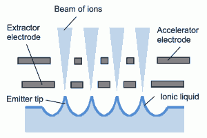
Electrospray is a process to ionize electrically conductive liquids that relies on strong electric fields; charged particles are emitted from sharp tips that serve as field enhancers to increase the electrostatic pressure on the surface of the liquid, overcome the effects of surface tension, and facilitate the localization of emission sites. Ions can be emitted from the liquid surface if the liquid is highly conductive and the emitter flowrate is low. Previous research demonstrated successful operation of massive arrays of monolithic batch-microfabricated planar electrospray arrays with an integrated extractor electrode using ionic liquids EMI-BF4and EMI-Im [] [] – liquids of great importance for efficient nanosatellite propulsion. The current work aims to build upon the previous electrospray array designs by increasing the density of the emitter tips, increasing the output current by custom-engineering suitable nanofluidic structures for flow control, and improving the ion optics to gain control of the plume divergence and exit velocity.
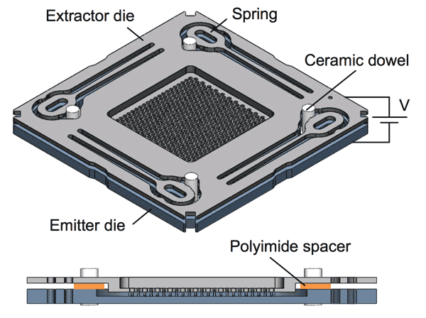
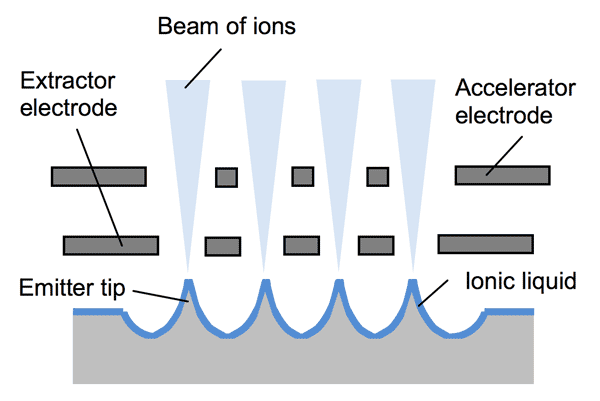
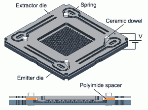
The basic version of the MEMS electrospray array consists of an emitter die and an extractor die (shown in Figure 1), both made of silicon and fabricated using deep reactive ion etching. The two dies are held together using a MEMS high-voltage packaging technology based on microfabricated springs that allows precision packaging of the two components with less than 1% beam interception [] [] . The emitter die contains dense arrays of sharp emitter tips with as many as 1,900 emitters in 1 cm2. A voltage applied between the emitter die and the extractor electrode creates the electric field necessary to ionize the ionic liquid (see Figure 2). A nanostructured material transports the liquid from the base of the emitters to the emitter tips. The present research focuses on engineering the nanofluidic structure to attain higher emitter current while maintaining good array emission uniformity and on developing batch microfabricated advanced ion optics to control the electrospray plume.
-
-
Figure 1: Design of the basic version of the MEMS electrospray array, consisting of an emitter die and an extractor die.
-
-
Figure 2: Schematic of externally fed electrospray emitter tips and the electrodes that create an electric field to produce a beam of ions.
- Authors: P. J. Ponce de Leon, F. Hill, L. F. Velásquez-García
- Sponsorship: DARPA
Electrospinning is a process in which a membrane-like web of thin fibers can be produced using high electrostatic fields and polar liquids with high viscosity. It is the only known technique that can generate continuous fibers with controlled morphology in the 10-500 nm diameter range and has tremendous versatility as it can create non-woven or well-aligned mats of polymer, ceramic, semiconductor, and/or metallic fibers using the same hardware. Electrospinning is also capable of conformally coating 3D complex shapes with ultrathin layers that have complex multi-layered structure and thickness variation across the surface. In particular, polymer electrospun fibers have been proposed to develop multi-stack functional fiber mats for protective gear, because they show high breathability, elasticity, and filtration efficiency. In addition, electrospun fibers made of the appropriate materials could also be used in flexible electronics (graphene) and in structural reinforcement against mechanical trauma. However, the production of electrospun nanofibers has very low throughput due to the small fiber diameter, which limits their applications to high-end products. In this project we are investigating the development of high-throughput electrospun nanofibers using batch-microfabricated arrays of externally fed electrospinning emitters. Externally-fed emitters are attractive, because they do not require high pressure drops as internally-fed emitters do. Also, they do not clog and can process liquids that bubble.
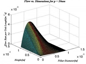
An aspect of this project is looking into the physics of wicking to optimize the fluidic micro/nanostructures that control the emitter flow rate. For solids with intrinsic contact angles below some critical value determined by roughness geometry, it becomes energetically favorable for a droplet to completely impregnate the roughness and spread through it [] . This process of hemi-wicking has been described in pillar arrays of varying shapes and sizes [] [] . For externally-fed electrospinning, we must ensure a sufficient and steady flow rate of polymer solution to avoid broken or irregular fibers. We are theoretically and experimentally investigating optimal morphologies of both the micro/nano fluid control structures and the emitter geometry to attain good array emission uniformity.
-
-
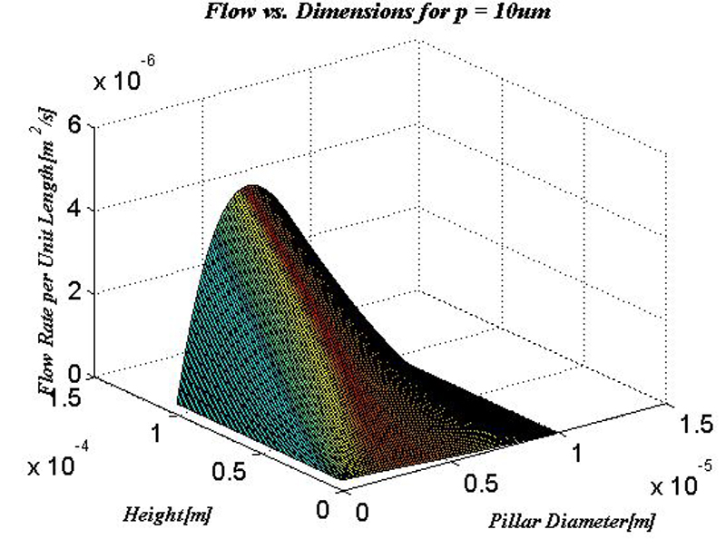
Figure 1: Fluid diffusion rate as a function of micropillar height and diameter for a fixed pitch of 10 µm. At constant height, there exists some intermediate diameter where the flow is maximized.
-

-
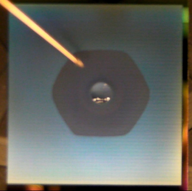
Figure 2: Photograph of fluid being transported through the micropillar patterned surface. Several different spreading regimes can be achieved by varying micropillar geometry.