- Authors: F. Niroui, A. Wang, T. Andrew, V. Bulovic, J. H. Lang
- Sponsorship: NSF
Polymer materials doped with conductive particles exhibit piezoresistive properties. These materials are fabricated such that their conductivity changes with an applied compressive force. When compressed, the formation of percolation pathways allows increased electrical conduction through tunneling between the particles. This work explores and utilizes this property of composites to fabricate various devices with the ultimate goal of developing integrated flexible systems resembling sensory skins.
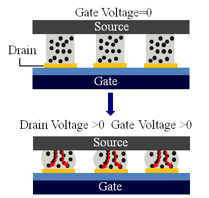
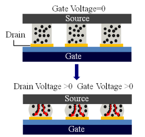
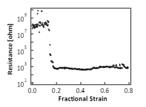
As a first generation of piezoresistive devices, a squeezable switch (squitch) is fabricated with a three-terminal configuration shown in Figure 1 [] . In this study, the squitch is fabricated from a composite of polydimethylsiloxane doped with 60 wt% Ni microparticles that shows more than 5 orders of magnitude change in conductivity over a 20% strain (Figure 2). In the absence of an applied gate bias, the composite is a poor conductor. An applied gate voltage generates an electrostatic force between the source and the gate that compresses the composite, causing the squitch to conduct. To allow fabrication of reliable and reproducible devices, the composite needs to be engineered such that its mechanical properties are more stable. To achieve this goal, current research explores the effects of the type of polymer and conductive particles and the method of fabrication on the properties of the nanocomposite and performance of the squitch. The surfaces of the metal particles are chemically treated to allow better distribution in the polymer matrix while also chemically binding the particles to the polymer preventing particle migration over repeated use of the device. After the composite is optimized, future work will involve extending the squitch design to fabricate devices such as analog amplifiers, digital inverters, and various sensors and developing processes to allow large-area fabrication. The devices will then be integrated to develop artificial skins.
-
-
Figure 1: Operation mechanism of the squitch.
-
-
Figure 2: Resistance change in Ni-PDMS composite due to an applied compressive force.
- Authors: A. Wang, T. L. Andrew, F. Niroui, A. Murarka, V. Bulović, J. H. Lang
- Sponsorship: NSF Center for Energy Efficient Electronics Science
Nano-electromechanical systems (NEMS) are an emerging area of research with potential applications as low-power switches for electronic circuits. The proliferation of electronics in both stationary and portable applications demands the development of more energy-efficient devices than are currently available. While solid-state silicon MOS-based transistor circuits, the dominant technology in today’s electronics, have greatly reduced their power requirements by aggressive scaling, the concurrent increase in off-state leakage current limits their energy efficiency. In contrast, microelectromechanical relays have been demonstrated with zero off-state currents and abrupt switching characteristics [] [] . As these and other electromechanical devices are shrunk to the nanoscale, their actuation voltages, and hence power requirements, are expected to be reduced significantly.
Our group recently presented a three-terminal electromechanical switch based on a piezoresistive polymer nanocomposite as the active material [] . The metal-polymer composite consisted of a polydimethylsiloxane polymer matrix doped with 60 wt% nickel particles. A schematic diagram of this squeezable switch, or “squitch,” is shown in Figure 1. In its initial state, the conductive metal particles are separated by the insulating polymer matrix. Thus, the active material is highly resistive, and little current flows through the device (in the “off” state). When compressed, the metal-metal distances decrease until the onset of tunneling allows current to flow from source to drain (“on” state). The first-generation squitch demonstrated transistor-like behavior with drain-source conduction modulation over 4 orders of magnitude when electromechanical force was applied. However, the large mechanical dimensions of this concept demonstration necessitated higher supply voltages than desired. Our current work focuses on incorporating the squitch concept into nanoscale devices by (a) developing improved device structures and fabrication methods and (b) exploring new materials such as ligand-coated nanoparticles and self-assembled monolayers as active materials.

Figure 1: Schematic diagram of squitch. Applying a voltage bias between gate and source generates an electrostatic force that compresses the active material and allows carriers to tunnel from source to drain. When the voltage bias is removed, the active material acts as a mechanical spring and recovers from its compressed state to cut off current flow through the device.