- Authors: A. Al-Obeidi, C. V. Thompson
- Sponsorship: Singapore-MIT Alliance for Research and Technology
Micro-batteries provide a critical component for self-powered autonomous microsystems. Lithium-ion batteries provide relatively high energy storage capacities. Significant improvement in energy storage capacities over current generation lithium-ion batteries is achievable by using silicon as the anode material. Silicon has the highest known Li capacity, up to 4.4 lithium atoms per silicon atom. However, lithiation of silicon results in large volume changes that cannot be sustained in monolithic forms such as fully dense films or substrates. To employ silicon-based lithium batteries, nanostructured silicon nanowires with high surface-to-volume ratios and superior mechanical properties over bulk are being investigated [] [] .
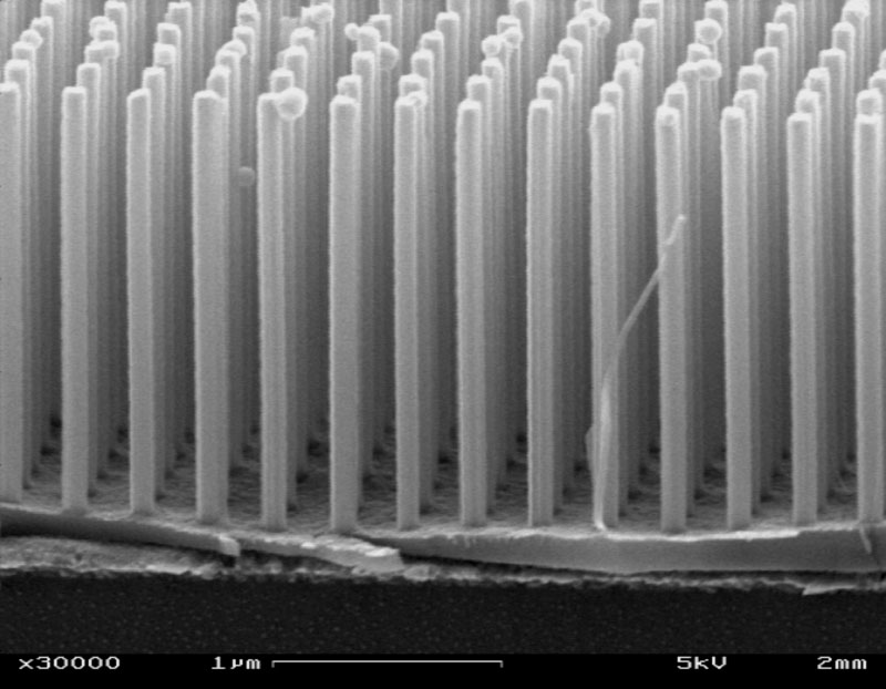
We use metal-catalyzed etching (MCE) to fabricate the silicon nanowires, a process that offers low-cost, room temperature processing of silicon. The process takes advantages of a thin, patterned metal film that catalyzes the etching of silicon when immersed in an HF solution with an oxidant such as H2O2. MCE can be used to create of large (>1 cm2) arrays of perfectly ordered Si-NWs with periods down to 40 nm, diameters down to 20 nm, and aspect ratios up to 200 to 1 [] . These high-volume filling arrays are being used for studies of lithiation. Amorphous silicon-based nanowire arrays on various substrates are being explored for enhanced cyclability (Figure 1).

Figure 1: Amorphous silicon nanowires on glass using MCE [] . These wires are expected to better accommodate the stresses associated with lithiation.
- Authors: A. Al-Obeidi, H. Zhao, C. V. Thompson
- Sponsorship: International Iberian Nanotechnology Laboratory
Silicon nanowires (NWs) have attracted immense interest for sensing applications due to their high surface-to-volume ratio. In particular, field-effect-based chemical sensors are an attractive platform for fabricating multi-channel analysis systems capable of detecting bio-molecule concentrations and enzyme reactions. One can measure the concentrations of target analytes by taking advantage of changes in either capacitance or conductivity due to binding of chemical and biological species to the NW surface. However, most nanowire-based biochemical sensor studies employ planar field-effect transistor (FET) structures. In comparison, vertical freestanding FET structures sensors have a greater potential for ultrahigh sensitive detection because of the still larger exposed surface interaction area in high density arrays.
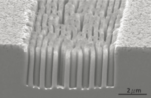
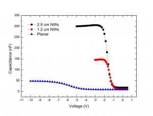
One solution to fabricating vertically aligned FETs is through metal-catalyzed etching (MCE) [] [] , a low-cost, room temperature method which enables fabrication of highly ordered Si NW arrays of large aspect ratios (Figure 1). Such structures are very promising for the detection of multiple targets in an integrated microfluidic system. Improvement in sensor sensitivity using an electrolyte-semiconductor-silicon (EIS) sensor system was found to scale with nanowire length, translating into a stronger sensor signal when compared to a planar EIS sensor (Figure 2).
-

-
Figure 1: Vertical silicon nanowire arrays in channels using metal- catalyzed etching.
-

-
Figure 2: C/V curves for planar and NW-based EIS sensors. Enhancement in capacitance, or effective sensors signal, scales with increasing surface area. Signal enhancement was 3 times and 6 times that of the planar system for the short and long nanowire systems, respectively.
- Authors: W. Zheng, A. Al-Obeidi, C. V. Thompson
- Sponsorship: SRC
Capacitors with high capacitance density (capacitance per footprint area) have potential applications in autonomous microsystems and for power management in high performance integrated circuits. For self-powered autonomous systems, batteries are needed for storage of harvested energy with high energy densities. However, batteries are limited in their discharge power. Coupled with capacitors, stored energy can be released at high powers, e.g., for broadcast of data. Supercapacitors can also be used in on-chip switched capacitor converters for dynamic voltage scaling in low power integrated circuits [] .
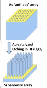
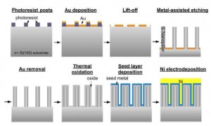
We are investigating the use of silicon nanowire arrays for fabrication of on-chip supercapacitors. To fabricate nanowire arrays, we are using metal catalyzed etching (MCE) (Figure 1). This is a room temperature wet etching process that has been used to create arrays of nanowires with radii and spacing in the range of tens of nanometers, with wire aspect ratios of over 200 to 1 [] .
In earlier work, we demonstrated the feasibility of using the MCE to fabricate Si nanowires to make supercapacitors (Figure 2) [] . We have demonstrated a factor of approximately 10 times improvement in the capacitance density over planar devices for nanocapacitors with a 200-nm period and 1.5-μm height. Further improvement of silicon nanowire capacitors can be achieved by optimizing the geometries of the nanowire arrays and the dielectric material and structure, as well as the device layout. Our current work has focused on improving the capacitor performance by decreasing the equivalent series resistance. Lower resistance will provide a higher AC effective capacitance density and less heat generation. Two approaches are under investigation to reduce the series resistance. One is through improved design of nanocapacitor arrays; the other is conversion silicon nanowires to silicide nanowires.
-

-
Figure 1: Scheme of the MCE process.
-

-
Figure 2: Schematic nanocapacitor process flow.
