A Low-power SAR ADC with Redundancy
- Category: Circuits & Systems
- Tags: albert chang, duane boning, hae-seung lee
Technology scaling has enabled low-power operations in digital integrated circuits. Therefore, the trend to move analog-to-digital operations upstream to allow more signal-processing to shift from the analog domain to the digital domain is inevitable. As most real world signals remain analog, the design of high-performance and low-power analog-digital converters (ADC) plays a key role in the success of future integrated system design. In this research, we focus on designing a (1) robust, (2) low-power, and (3) high-performance time-interleaved successive-approximation-register (SAR) ADCs. The SAR architecture is adopted because of its good digital compatibility and high energy efficiency while achieving high sampling rates.
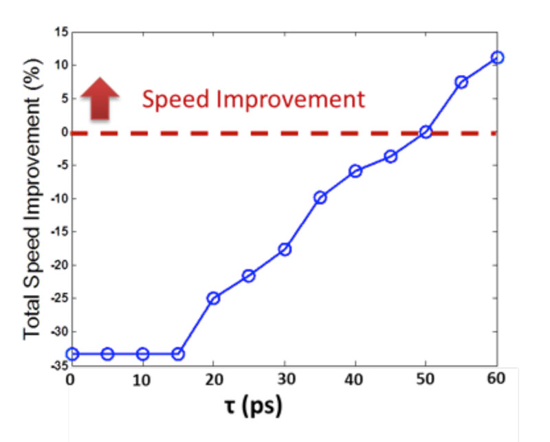
The robustness of SAR ADCs is achieved by analyzing the effectiveness of redundancy (digital error correction) [1] [2] in improving sampling rates and its immunity from incomplete bit-settling errors. Analysis shows that the redundancy algorithm does not help improve sampling rate in all SAR ADC designs; instead, the maximum sampling rate depends on the settling time constant (τ) and the relative magnitude of the ADC delay components [3] . As shown in Figure 1, in order to benefit from redundancy algorithm, τ has to be more than 50ps.
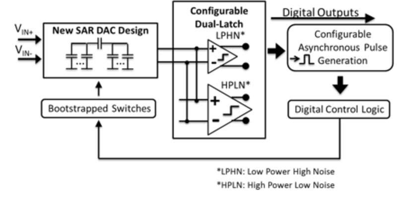
The low-power operation is achieved by combining the merged capacitor switching algorithm [4] and split capacitive array [5] . The merged capacitor-switching algorithm suffers from its sensitivity to the parasitic capacitance on the outputs of the capacitive DAC. The split capacitive array suffers from 4x loss in signal power to keep voltage below the supply rail on the sub-DAC and from the mismatch problem between the fractional bridge capacitor to other capacitors in the DAC. Both issues are researched and resolved in our design. A new digital calibration scheme is developed to digitally calibrate the ADCs to resolve the mismatches and parasitic issues. Our design also incorporates an asynchronous on-chip pulse generator to avoid synchronous high-power clock distribution circuit on-chip. The overall SAR ADCs architecture is depicted in Figure 2.
- F. Futtner, “A 1.2V 10b 20MSample/s non-binary successive approximation ADC in 0.13μm CMOS,” in IEEE International Solid-State Circuit Conference Digest of Technical Papers, 2002, pp. 136-137. [↩]
- T. Ogawa, H. Kobayashi, M. Hotta, Y. Takahashi, H. San, and N. Takai, “SAR ADC Algorithm with redundancy,” in IEEE APCCAS, pp. 268-271, Nov. 2008. [↩]
- A. H. Chang, H.-S. Lee, and D. S. Boning, “Redundancy in SAR ADCs,” in Great Lakes Symposium on VLSI, May 2011. [↩] [↩]
- V. Hariprasath, J. Guerber, S.-H. Lee, and U.-K. Moon, “Merged capacitor switching based SAR ADC with highest switching energy-efficiency,” Electronics Letters, vol. 46, pp. 620-621, Apr. 2010. [↩]
- Y. Chen, X. Zhu, H. Tamura, M. Kibune, Y. Tomita, T. Hamada, M. Yoshioka, K. Ishikawa, T. Takayama, J. Ogawa, S. Tsukamoto, and T. Kuroda, “Split capacitor DAC mismatch calibration in successive approximation ADC,” in IEEE Custom Integrated Circuits Conference, 2009, pp. 279 –282. [↩]