Templated Placement of Colloidal Quantum Dots
Semiconductor quantum dots (QDs) are electronically-quantized systems with promising applications in optoelectronic devices [1] . A key aspect of such systems is the fine control of optical transitions in the synthesis process [2] . These QDs are predominantly used in thin-film arrangement, deposited by spin casting or dip coating. Single QD patterning is one of the major challenges to designing a system that takes advantage of individual properties of QDs. Here we present a template self-assembly technique to control the position of individual QDs through electron-beam lithography (EBL). This optimized top-down lithographic process is a step towards the integration of individual QDs in optoelectronics systems for industrial applications.
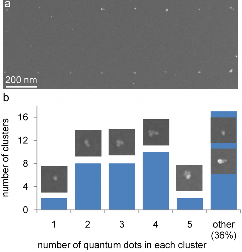
The fabrication process of templated QDs is illustrated in Figure 1a. A poly(methylmethacrylate) (PMMA) resist was spin coated on a silicon substrate, followed by the fabrication of a mask through EBL. The size of the resulted PMMA templates was minimized by varying development temperature [3] [4] . Figure 1b shows the optimized PMMA patterning, with minimum template (i.e., hole) size of 8 nm for development at 6 °C. After defining the PMMA templates, a solution of QDs (6-nm-diameter CdSe) was spin casted and the remaining resist was removed by dissolution in acetone. This process resulted in QD clusters attached on the substrate. By optimizing the QD solution concentration, resist thickness, and feature size, we fabricated clusters with 1 to 10 QDs. One figure of merit in this process is the pattern yield, which is the ratio of yielded structures to the patterned templates. Figure 2 shows QD clusters with 87% pattern yield, with an average of 3 QDs in each cluster. Control of QD placement will be further optimized and integrated into photonic devices.
-
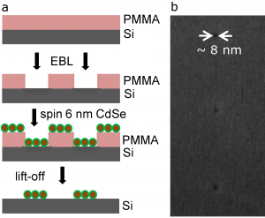
- Figure 1: (a) Fabrication process of templated QDs. PMMA was spin coated to a thickness of 40 nm on Si, followed by EBL. Then, 6 nm of CdSe QDs were spin coated. The PMMA lift off was done with acetone, leaving small clusters of CdSe QDs. (b) Scanning-electron micrographs of optimized PMMA templates with a minimum feature size of 8 nm for development at 6 °C.

-

- Figure 2: Scanning-electron micrographs of templated QDs (6-nm-diameter CdSe). The solution concentration was 2 µM and the PMMA thickness was 12 nm. (a) An overview of the pattern. (b) Histogram of the number of QDs in each cluster versus the number of clusters. We analyzed 54 clusters of QDs, and the QDs were counted by using high-resolution SEM micrographs. On the inset of every histogram bar is presented one illustrative SEM image used.
- A. P. Alivisatos, “Semiconductor clusters, nanocrystals, and quantum dots,” Science, vol. 271. no. 5251, pp. 933-937, Feb. 1996. [↩]
- S. A. Empedocles, D. J. Norris, and M. G. Bawendi, “Photoluminescence spectroscopy of single CdSe Nanocrystallite quantum dots,” Phys. Rev. Lett. vol. 77, pp. 3873-3876, Oct. 1996. [↩]
- W. Hu, K. Sarveswaran, M. Lieberman, and G. H. Bernstein, “Sub-10 nm electron beam lithography using cold development of poly(methylmethacrylate),” J. Vac. Sci. Technol. B vol. 22, pp. 1711-1716, June 2004. [↩]
- B. Cord, J. Lutkenhaus, and K. K. Berggren, “Optimal temperature for development of poly(methylmethacrylate),” J. Vac. Sci. Technol. B vol. 25, pp. 2013-2016, Dec. 2007. [↩]

