Synthesis of One- to Two-layer Hexagonal Boron Nitride Using Chemical Vapor Deposition
- Category: Materials
- Tags: Jing Kong, Ki Kang Kim, Tomas Palacios

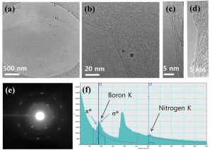
Figure 1: (a-d) Transmission electron microscopy images of one to two layers of hexagonal boron nitride (hBN) film, (e) Selective electron diffraction pattern of hBN film, (f) Electron energy loss spectra of hBN film.
Hexagonal boron nitride (hBN) is very attractive for a variety of applications, particularly as deep ultraviolet emitter, transparent membrane, dielectric layer/substrate, or protective coating. In this work, we carried out detailed investigation of hBN synthesis on Cu substrate using chemical vapor deposition (CVD) with two heating zones under low pressure (LP). Previously, few-layer hBN was synthesized via CVD under atmospheric pressure (AP) on metallic substrates [1] [2] . In contrast, one- or two-layer hBN is synthesized under LPCVD. Ammonia borane, which is easier accessible and more stable in the atmosphere than borazine, is used as a BN precursor. These mono- or bi-layer hBN films are characterized by atomic force microscopy, transmission electron microscopy and electron energy loss spectroscopy analyses. Our results suggest that the growth here occurs via surface-mediation, which is similar to graphene growth on Cu under low pressure. These atomically thin layers are particularly attractive for atomic membranes or dielectric layer/substrates for graphene devices.
- Y. M. Shi, C. Hamsen, X. T. Jia, K. K. Kim, A. Reina, M. Hofmann, A. L. Hsu, K. Zhang, H. N. Li, Z. Y. Juang, M. S. Dresselhaus, L. J. Li, and J. Kong, “Synthesis of few-layer hexagonal boron nitride thin film by chemical vapor deposition,” Nano Letters, vol. 10, pp. 4134-4139, Oct. 2010. [↩]
- L. Song, L. Ci, H. Lu, P. B. Sorokin, C. Jin, J. Ni, A. G. Kvashnin, D. G. Kvashnin, J. Lou, B. I. Yakobson, and P. M. Ajayan, “Large scale growth and characterization of atomic hexagonal boron nitride layers,” Nano Letters, vol. 10, pp. 3209-15, Aug. 2010. [↩]