Experiment and Simulation on Channel Mobility of In0.53Ga0.47As Quantum-well MOSFET Structures
- Category: Electronic Devices
- Tags: Eugene Fitzgerald, Li Yang
This paper discusses a way to optimize the In0.53Ga0.47As quantum-well MOSFET structures from the prospective of channel mobility. We experimentally demonstrated that the barrier thickness and interfacial defect density are two key factors determining the channel mobility, while the effect of the oxide charge is negligible. The mobility model consisting of phonon scattering and coulomb scattering was applied to fit the experimental data. According to the model, for quantum-well MOSFET structures with in-situ ALD Al2O3, the mobility is dominated by coulomb scattering for the thin barrier case (<5 nm) and dominated by phonon scattering for the thick barrier case (>5 nm). At a barrier thickness of 4 nm, compared to a structure with in-situ ALD Al2O3 with the mobility of 6807 cm2/Vs, which corresponds to an interfacial charged defect density of 1.1×1013 cm-2, the structure with in-situ CVD Al2O3 showed higher mobility (8883 cm2/Vs), which corresponds to a lower charged defect density (5×1012 cm-2).
-
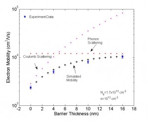
- Figure 1: Channel electron mobility versus the thickness of InGaAs/InAlAs barrier. The blue diamond symbols indicate the measured mobility. The magenta and red dots indicate the mobility limited by coulomb scattering and phonon scattering, respectively, and the black “+” symbols indicate the simulated final mobility.

-
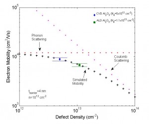
- Figure 2: Channel electron mobility versus the charged defect density. The blue diamond symbol and the green square symbol indicate the measured mobility for structure with CVD Al2O3/InGaAs interface and ALD Al2O3/InGaAs interface, respectively. The magenta and red dots indicate the mobility limited by coulomb scattering and phonon scattering, respectively, and the black “+” symbols indicate the simulated final mobility.
