Zinc Oxide Nanowire Devices

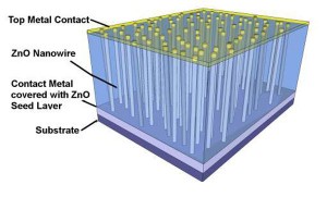
Figure 1: Design layout of a ZnO-nanowire-based touch sensor with vertically grown nanowires imbedded in a polymer matrix and sandwiched between top and bottom contacts.
Devices made utilizing zinc oxide (ZnO) nanowires have been developed for a variety of different applications including tactile sensors, flex sensors, transparent field-effect transistors (FETs), and ultra-violet (UV) sensors [1] [2]. Zinc oxide is an optically transparent, piezoelectric, piezoresistive, and direct wide-band-gap semiconducting material. By taking advantage of a sub-100°C hydrothermally based growth of ZnO nanowires, the devices can be made directly on flexible and transparent substrates in large areas and at low cost without the need for a transfer process [3]. The nanowires can be grown either in the vertical direction, normal to the substrate, or in the horizontal direction, in-plane with the substrate, depending on the device specifications and fabrication process. The tactile sensor devices developed are based on a cross-bar network comprising a top and bottom array of electrodes around a composite of vertically grown nanowires and an insulating polymer (Figure 1). This cross-bar network allows for individually addressable locations for tactile sensing based on the piezoelectric effect. The results for the tactile sensor show a clear spike in current when an insulating tip is placed on and removed from the surface [2]. These results are compared to control runs including a touch on the adjacent cross electrodes and testing devices without nanowires. Both tests show at least an order-of-magnitude difference in current between the control and the pressure sensor.
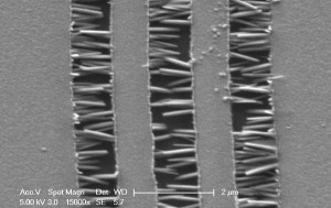
Growing ZnO nanowires in-plane to the surface at a low temperature can produce many new devices, including a single-nanowire FET and UV sensor (Figure 2). The combination of standard optical lithography and solution-based nanowire growth means that devices can be fabricated on a large scale. Initial results show promise that an in-situ single-nanowire UV sensor and FET can be achieved.
References
- Z. L. Wang, “Novel Nanostructures of ZnO for Nanoscale Photonics, Optoelectronics, Piezoelectricity, and Sensing,” Appl. Phys. A, vol. 88, pp 7 – 15, 2007. [↩]
- S. M. Pfaendler, M. E. Swanwick, A. R. Rachamim, P. Beecher, S. E. Machin, P. Andrew, W. I. Milne, and A. J. Flewitt, “A Large-area, Touch-sensitive Surface Comprising of a Zinc Oxide Nanowire Composite for Display Applications,” presented at 2009 MRS Fall Meeting, Boston, MA, December 2009. [↩] [↩]
- A. R. Rachamim, S. H. Dalal, M. E. Swanwick, A. J. Flewitt, and W. I. Milne, ” Quantitative Investigation of the Factors Affecting the Hydrothermal Growth of Zinc Oxide Nanowires,” presented at 2009 MRS Spring Meeting, San Francisco, CA, April 2009. [↩]
