Wafer Level CMP Modeling

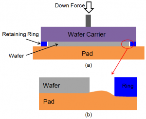
Figure 1: Wafer carrier configuration in CMP: (a) The wafer carrier holds the wafer facing down. The wafer is surrounded by a retaining ring, which is usually a few millimeters away from the edge of the wafer. (b) Pad deformation around the wafer edge.
The within-wafer non-uniformity of the material removal rate has long been a concern in chemical-mechanical planarization (CMP) [1]. Pressure distribution is known to be highly non-uniform near the wafer edge, which results in a typical edge roll-off profile [2] and reduces the yield of the process. The edge roll-off may result from the inherent discontinuities of the process tool geometry at the wafer edge. Figure 1(a) shows the wafer carrier configuration of a typical rotary CMP tool. The wafer is surrounded by a retaining ring. In a typical setting, different pressures are applied to the wafer and the ring, with the ring usually under higher pressure to prevent the wafer from slipping out. The pad bends around the wafer edge due to the existence of the gap and retaining ring as shown in Figure 1(b); thus the wafer edge is polished non-uniformly due to a localized pressure affected by the retaining ring. The factors causing the non-uniform pressure distribution include gap size, pad effective modulus, and reference pressures on the wafer and retaining ring.

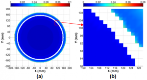
Figure 2: Pressure (MPa) distribution of 300-mm wafer in CMP with a retaining ring. The wafer reference pressure is 1 psi and the ring reference pressure is 4 psi. Pad modulus effective modulus is 100 MPa. The ring width is 20 mm. The gap between ring and wafer is 4 mm. (a) Whole-wafer pressure distribution. (b) Pressure distribution at wafer edge and ring edge.
To understand the non-uniform effect, we have built a physical wafer-level CMP model based on contact mechanics. The pad can be treated as an elastic body. Wafer and retaining ring are both rigid. When the wafer and ring are pressed to the pad, the relationship between pad deformation and wafer/ring surface topography can be simulated using a contact-wear model [3]. Figure 2 shows a simulation of 300-mm wafer surface pressure with a flat retaining ring. We see that the wafer-edge pressure is tuned by the retaining ring, and the high pressure region is on the ring. Current work is seeking to include detailed retaining ring surface structures (e.g. grooves in the ring) in the model.
References
- J. Luo and D. A. Dornfeld, Integrated Modeling of Chemical Mechanical Planarization for Sub-Micro IC Fabrication, Springer, Berlin (2004). [↩]
- X. Xie and D. Boning, “Modeling the Interaction Between Wafer Edge Geometry and Polish Performance,” Mat. Res. Soc. Symp. Proc., vol. 867, paper W.5.1.1 (2005). [↩]
- O. G. Chekina and L. M. Keer, “Wear-Contact Problems and Modeling of Chemical Mechanical Polishing,” J. Electrochem. Soc., 145, 2100 (1998). [↩]