Wafer-bonding Technology in Nitride Semiconductors

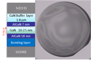
Figure 1: IR image of bonded GaN and Si wafers. The wafer diameter is 4”. The image in the left illustrates the bonded N-face sample structure.
GaN high-electron-mobility transistors (HEMTs) offer unprecedented high-voltage, high-power operation at RF frequencies due to their high band gap (3.4 eV) and electron mobility (1500-2000 cm2/Vs). Therefore, they are very promising for the next generation of highly efficient power amplifiers in RF base stations and radars.
The polar nature of GaN determines many of its properties. Depending on the polarity of the GaN surface, GaN is termed Ga-face or N-face. Currently most GaN HEMTs are made with Ga-face grown material because it is difficult to grow high-quality GaN in N-face. However, N-face GaN HEMTs would offer numerous benefits such as low contact resistance and a natural back barrier.

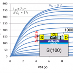
Figure 2: Output characteristics of a fusion bonded N-face GaN transistor. The inset depicts the device structure.
Previously N-face GaN HEMTs with high-quality Ga-face grown material have been demonstrated with bonding technology [1]. However, the demonstration had several shortcomings such as low transconductance and high contact resistance due to the large distance between the gate and the 2DEG channel. Also the bonding technology was demonstrated only for pieces. For the bonding technology to be a commercially viable, wafer-level bonding has to be demonstrated.
This project focuses on demonstrating a wafer-level bonding technology for GaN, as well as developing new epi-structures to take full advantage of the new flexibility offered by N-face GaN. The wafer-level bonding developed in this project employs chemical-vapour-deposited- (CVD) grown oxide and chemical-mechanical polishing (CMP) to smooth the surface of the GaN layer to enable fusion bonding of the GaN wafer to Si carrier wafer. Also a selective dry etch based on SF6/BCl3 plasma has been developed that allows the use of thin AlGaN etch-stop layers to precisely control the remaining GaN thickness for the channel. By combining all these technologies, the project aims to demonstrate state-of-the-art GaN HEMTs with unprecedented power output at RF frequencies.
References
- J. Chung, E. Piner, and T. Palacios, “N-Face GaN/AlGaN HEMTs Fabricated Through Layer Transfer Technology,” Electron Device Letters, IEEE, vol. 30, 2009, pp. 113-116. [↩]