W-band GaN Transistors and their Integration with Si(100) Electronics

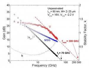
Figure 1: RF performance of unpassivated 60-nm gate length HEMT showing fT = 70 GHz and fmax = 300 GHz. The fT and fmax values are extrapolated following a -20 dB/dec ideal decrease with frequency.
GaN-based high-electron-mobility transistors (HEMTs) have become one of the prime candidates for solid-state power amplifiers at frequencies above 30 GHz. To maximize the performance of GaN HEMTs at millimeter-wave frequencies (30-300 GHz), one of the key challenges is to increase the power-gain cut-off frequency (fmax). In this project, we have obtained state-of-the-art fmax in GaN HEMTs by combining low-damage gate recess technology, scaled device geometry, and recessed source/drain ohmic contacts to simultaneously enable minimum short-channel effects (i.e., high output resistance, Rds) and very low parasitic resistances. A 60-nm gate-length HEMT with recessed AlGaN barrier exhibited excellent Rds of 95.7 Ω·mm, Ron of 1.1~1.2 Ω·mm, and fmax of 300 GHz (Figure 1) with a breakdown voltage of ~20 V [1]. To the authors’ knowledge, the obtained fmax is the highest reported to date for any nitride transistor.

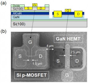
Figure 2: (a) A cross-section schematic of fabricated Si p-MOSFETs and GaN HEMTs. (b) A plan-view SEM image of the fabricated transistors.
Our group is also working on the on-wafer integration of these high-performance GaN devices with silicon (100) CMOS electronics. A robust heterogeneous integration technology would make the outstanding analog and mixed-signal performance of GaN electronics available to Si VLSI chips. We have recently demonstrated the first integration of Si(100) MOSFETs and GaN HEMTs on the same wafer in very close proximity [2]. To enable a fully Si-compatible process, we fabricated a novel Si(100)-GaN-Si(100) virtual substrate through a wafer-bonding and etch-back technique. The high thermal stability of nitride semiconductors allowed the fabrication of Si MOSFETs on this substrate without degrading the performance of the GaN epilayers. After the Si devices were fabricated, the nitride epilayer was exposed and the nitride transistors were processed. Using this technology, GaN and Si devices separated by less than 5 µm from each other have been fabricated (Figure 2). This configuration is suitable for building future heterogeneous integrated circuits.
References
- J. W. Chung, W. E. Hoke, E. M. Chumbes, and T. Palacios, “AlGaN/GaN HEMT with 300 GHz fmax,” IEEE Electron Device Lett., vol. 31, no. 3, pp. 195-197, Mar. 2010. [↩]
- J. W. Chung, J. Lee, E. L. Piner, and T. Palacios, “Seamless On-wafer Integration of Si(100) MOSFETs and GaN HEMTs,” IEEE Electron Device Lett., vol. 30, no. 10, pp. 1015-1017, Oct. 2009. [↩]