Ultra-high-speed Zero-Crossing-based ADC
With an increasing need for higher data rates, both wireless applications and data links are demanding higher speed analog-to-digital converters (ADC) with medium resolution. In particular, this work investigates ADCs with sampling rate up to 2 Gs/s with 6-8 bits of resolution.
Time-interleaved converters achieve their high sampling rate by placing several converters in parallel. Each individual converter, or channel, operates at a reduced sampling rate and is responsible for digitizing a different time slice. This method requires matching of the individual converters, which make up the parallel combination. Therefore channel-matching is an important design consideration for time-interleaved ADCs.
Although digital calibration can mitigate many of these non-idealities, timing mismatch is a non-linear error that is more difficult to remove. At sampling rates up to 2Gs/s, digital calibration would consume a large amount of power. An alternative solution uses a global switch running at the full sampling speed of the converter. Although this technique works reasonably well for medium-high speed ADC’s [1] [2] , its effectiveness is limited by parasitic capacitance. We have developed a double-global sampling technique to remove the effect of parasitic capacitance on timing skew. At higher speeds the ability to turn the switch on and off at the full sampling rate becomes a major challenge. However, the use of scaled CMOS technology and gate-boosted switches still enables multi-GHz input bandwidth.
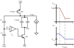
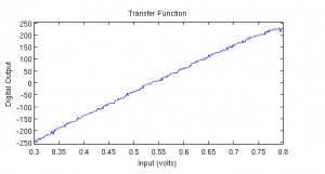
Power optimization is a major design consideration when implementing a time-interleaved ADC. We will lower total power consumption by exploring innovative technologies for implementing the individual ADCs in the channel, such as the zero-crossing-based circuit (ZCBC) topologies previously presented. In particular, this work is investigating a fast, single-slope architecture (Figure 1). The primary emphasis is the development of high-speed, highly power efficient single-slope ZCBC architecture. Since the single slope architecture is more sensitive to non-idealities such as ramp nonlinearity, we have carefully studied the sources of non-idealities and developed techniques to address the accuracy issues. Figure 2 shows the preliminary results. The performance of the system is limited by digital noise coupling and non-linearity.
References

