Top-down Fabrication of AlGaN/GaN Nanowires

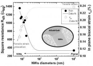
Figure 1: Square resistance and in-plane biaxial strain as a function of NWs’ diameter. The inset shows a scanning electron microscopy image of NWs with d~70 nm.
The frequency performance of
AlxGa1–xN/GaN high-electron-mobility transistors (HEMTs) has rapidly increased in recent years. Transistors with current gain cut-off frequencies (fT) above 160 GHz and power gain cut-off frequencies (fmax) of more than 300 GHz have been reported [1] [2]. In spite of these excellent results, the frequency performance of these devices is still far from their theoretical limit. In this project, we are developing nanowire-based nitride HEMTs to overcome these limitations and to explore the maximum frequency of nitride devices [3].

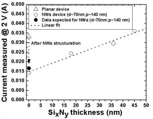
Figure 2: Current measured in TLM devices as a function of SixNy thickness deposited by CVD. The black solid point is the expected value for the current when taking into account the AlGaN/GaN material removed during the fabrication of the NWs (d~70 nm and pitch ~ 140 nm).
Top-down fabrication of horizontal AlGaN/GaN nanowires (NWs) has been performed on planar AlGaN/GaN samples grown on a silicon substrate. E-beam lithography and Cl2-based dry-etching were used to define nanowires with diameters (d) in the 30-200-nm range. The transmission line method (TLM) and visible Raman spectroscopy were used to characterize the NWs as well as planar devices. Figure 1 shows the square resistance (Rsq) and in-plane biaxial strain (exx) in the NWs as a function of diameter [4]. The Rsq increases exponentially when the NWs’ diameter is reduced. This behavior can be explained by the tensile strain relaxation occurred during the NWs’ fabrication [5]. To improve the NWs’ conductivity (d<100 nm), silicon nitride (SixNy) was deposited by chemical vapor deposition (CVD) on NWs. Figure 2 shows the current measured in TLM devices as a function of SixNy thickness. A linear increase of the current occurs when the SixNy thickness increases. For an optimal SixNy thickness of 45 nm, the current measured through the horizontal assembly of NWs is 8% higher than in planar devices. The characterization of the high-frequency performance of these nanowires is currently underway. It is expected that the large carrier confinement of these devices will allow higher operating frequencies as well as linearity.
References
- T. Palacios, A. Chakraborty, S. Heikman, S. Keller, S. P. DenBaars, and U. K. Mishra, “AlGaN/GaN high electron mobility transistors with InGaN back-barriers,” IEEE Electron Device Lett., vol. 27, no. 1, pp. 13-15, Jan. 2006. [↩]
- J. W. Chung, W. E. Hoke, E. M. Chumbes, and T. Palacios, “AlGaN/GaN HEMT with 300-GHz fmax,” IEEE Electron Device Lett., vol. 31, no. 3, pp. 195-197, Mar. 2010. [↩]
- Y. Li, J. Xiang, F. Qian, S. Gradecak, Y. Wu, H. Yan, D. A. Blom, and C. M. Lieber, “Dopant-Free GaN/AlN/AlGaN radial nanowire heterostructures as high electron mobility transistors,” Nano Lett., vol. 6, pp 1468–1473, 2006. [↩]
- S. Tripathy, S. J. Chua, P. Chen and Z. L. Miao, J. Appl. Phys. 92, 3503 (2002). [↩]
- Y. Zhang, I. P. Smorchkova, C.R. Elsass, S. Keller, J. P. Ibbetson, S. Denbaars, U. Mishra, and J. Singh, J. Appl. Phys. 87, 7981 (2000). [↩]