Thermal Imaging Microscopy of Semiconductor Devices
The thermoreflectance (TR) technique, shown in Figure 1(a), is utilized to examine thermal conductivity of 0.6% ErAs: N-type InGaAlAs thermoelectric elements with a thickness of 60 um and an area of 1 mm by 1 mm. By monitoring the small fractional change in the reflectance of blue light occurring when the temperature of the surface is modulated, we can achieve submicron spatial resolution and a temperature resolution of 10 mK [1]. In this experiment, the temperature gradient is created by a thermoelectric heater/cooler while the heat flux is measured with thermocouples. The temperature profile across the sample is shown in Figure 1(b). The non-linear temperature profile indicates that the thermal conductivity has changed across the sample during the long (24 hours) molecular beam epitaxy (MBE) growth of the sample. The Al concentration could potentially explain the variation in thermal conductivity. Since any scratches or defects could introduce spurious noise and therefore errors to TR measurements, infrared (IR) lock-in thermography is further used to verify the data.
IR lock-in thermography [2], shown in Figure 2(a), is used to detect radiation in the infrared range of the electromagnetic spectrum and produce images. Because of the long wavelength of 3-5 um, the spatial resolution of IR lock-in thermography is limited to the micron range. A Cassegrain objective, a combination of concave and convex mirrors coated with gold, is selected for this long wavelength range. Similar to Figure 1(b), Figure 2(b) shows a non-linear temperature profile with low spatial resolution due to the diffraction limit. The minimal thermal conductivity is 30 percent lower than the average, which means we could underestimate ZT by 60 percent.
-
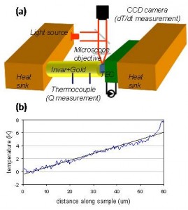
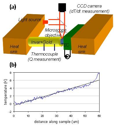
- Figure 1: (a) Schematic diagram of thermoreflectance (b) TR image of 0.6% ErAs: N-type InGaAlAs.
-
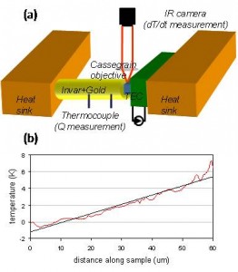
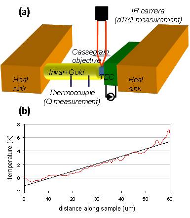
- Figure 2: (a) Schematic diagram of IR lock-in thermography (b) IR image of 0.6% ErAs: N-type InGaAlAs.
References
- P. Mayer et al., “Theoretical and experimental investigation of the resolution and dynamic range of CCD-based thermoreflectance imaging,” Journal of the Optical Society of America A, 24, 1156-1163 (2007). [↩]
- S. Huth et al., “Lock-in IR-thermography—a novel tool for material and device characterization,” Solid State Phenomena, 82–84, 741–746 (2002). [↩]
Filed under: Optics & Photonics |
Tags: katey lo, rajeev ram
![]() Print This Page
Print This Page
![]() Download as PDF
Download as PDF