Templated Self-assembly of Block Copolymers for Nanolithography

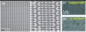
Figure 1: (a and b) SEM images of highly organized and asymmetric complex cylindrical BCP patterns with an array of HSQ posts (brighter dots) prepared by electron-beam patterning. (a) Zig-zag pattern and (b) Meander structure with sharp bends. (c and d) Sub-10-nm-wide (a) PDMS pattern and their pattern transfer to (b) sub-10-nm tungsten nanowires.
Self-organized macromolecular materials can provide an alternative pathway to conventional lithography for the fabrication of devices on the nanometer scale. In particular, the self-assembly of the microdomains of diblock copolymers within lithographically-defined templates to create patterns with long range-order has attracted considerable attention, with the advantages of cost-effectiveness, large-area coverage, and compatibility with pre-established top-down patterning technologies. Block copolymers consist of two covalently bound polymer chains of chemically distinct polymer materials. The chains can self-assemble to form small-scale domains whose size and geometry depend on the molecular weights of the two types of polymer and their interaction.

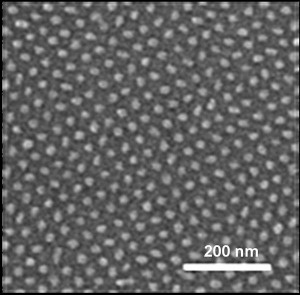
Figure 2: Square array of PFS dots from a thin film of PI-b-PS-b-PFS triblock terpolymer. PI and PS have been removed by O2 RIE.
Previously, we showed that spherical morphology poly(styrene-b-dimethylsiloxane) (PS-PDMS) block copolymers, which have a large interaction parameter and a high etch-contrast between two blocks, can be templated using an array of nanoscale topographical elements that act as surrogates for the minority domains of the block copolymer [1]. Recently, we showed that complex nanoscale patterns can be generated by combining the self-assembly of block-copolymer thin films with minimal top-down templating. A sparse array of nanoscale HSQ posts was used to accurately dictate the assembly of a cylindrical PS-PDMS diblock copolymer into a wide assortment of complex, unsymmetrical features, as shown in Figure 1(a) and (b) [2]. To extend the feature sizes to the sub-10-nm range, we demonstrated the formation of highly ordered grating patterns with a line width of 8 nm and a period 17 nm from a self-assembled PS-PDMS diblock copolymer. Sub-10-nm-wide tungsten nanowires were fabricated from the self-assembled patterns using a reactive ion etching process, as shown in Figure 1(c) and (d).
Beyond the rather limited morphologies of diblock copolymers, ABC triblock polymer thin films provide a diversity of new structures. For example, we obtained high-density nano-ring structures from a core-shell structured PS-PFS-P2VP triblock terpolymer after the selective removal of PS and P2VP [3]. Square arrays of dots can also be achieved from a self-assembled PI-PS-PFS triblock terpolymer, as shown in Figure 2 [4].
References
- I. Bita, J.K.W. Yang, Y.S. Jung, C.A. Ross, E.L. Thomas, and K.K. Berggren, “Graphoepitaxy of self-assembled block copolymers on two-dimensional periodic patterned templates,” Science, vol. 321, pp. 939-943, 2008. [↩]
- J.K.W. Yang, Y.S. Jung, J.-B. Chang, C.A. Ross, and K.K. Berggren, “Complex self-assembled patterns using sparse commensurate templates with locally varying motifs,” Nature Nanotechnology, vol. 5, pp. 256-260, 2010. [↩]
- V.P. Chuang, C.A. Ross, J. Gwyther, and I. Manners, “Self-assembled nanoscale ring arrays from a polystyrene-b-polyferrocenylsilane-b-poly(2-vinylpyridine) triblock terpolymer thin film,” Adv. Mater. vol. 21, pp. 3789-3793, 2009. [↩]
- V.P. Chuang, J. Gwyther, R.A. Mickiewicz, I. Manner, and C.A. Ross, “Templated Self-Assembly of Square Symmetry Arrays from an ABC Triblock Terpolymer,” Nano Lett., vol. 9, pp. 4364-4369, 2009. [↩]