Sub-5 keV Scanning-Electron-Beam Lithography
Scanning-electron-beam lithography (SEBL) commonly uses voltages between 10-100 keV. Higher voltages result in distributed proximity effects, lower sensitivity, and a higher probability of substrate damage. Proximity effects raise concern because these effects limit resolution at voltages 10-50 keV and complex and computationally-intensive programs are used to correct such effects. Proximity effects can be reduced by using either very high voltages (100 keV) or very low voltages around 1 keV [1]. Our research efforts have investigated the feasibility of SEBL at energies of 2 keV and below.
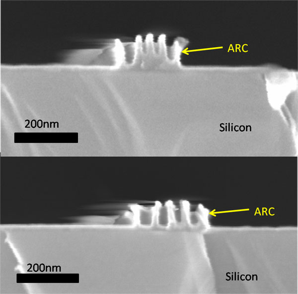
Nested Ls patterned in 15-nm-thick hydrogen silsesquioxane (HSQ) on silicon were used to investigate the resolution limit for dense patterns at low-voltages. Ls at 20-nm pitch were sucessfully patterned at energies of 2 keV and 1.5 keV, as shown in Figure 1. At 1 keV energy, the finest pitch possible was 25 nm. Nested Ls were also patterned in 11-nm-thick poly methyl methacrylate (PMMA) on silicon, with the minimum resolvable pitch at an energy of 2 keV being 70 nm. Monte-Carlo simulations of point-spread and line-spread functions were performed for a 2 keV, 9-nm diameter electron-beam incident on 15-nm-thick HSQ on silicon. The simulated distributed-energy-profile of dense Ls is in agreement with experimental results. To demonstrate pattern-transfer capability of patterns fabricated with low-voltage SEBL, dense line patterns in HSQ were reactive-ion-etched (RIE) into XHRiC anti-reflective layer with HSQ as the etch mask.
-
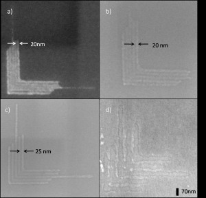
- Figure 1: Scanning-electron micrographs of nested Ls in 15-nm-thick HSQ patterned at electron energies of a) 2 keV, b) 1.5 keV, and c) 1 keV. The samples were developed in salty developer (4%NaCl, 1%NaOH in de-ionized water) for 60s. d) Scanning electron micrograph of nested Ls in 11-nm-thick PMMA patterned at electron energy of 2 keV.

-

- Figure 2: Scanning-electron micrographs of XHRiC cross-sections after reactive-ion-etching for 50s. Electron-beam lithography at an energy of 2 keV was used to pattern HSQ with lines. The HSQ lines was then used as a mask to transfer the pattern into XHRiC. Top micrograph shows the successful pattern transfer with lines at a 30-nm pitch, and the bottom micrograph is a cross-section of lines at 40-nm pitch. The lines are roughly 9-nm wide and the XHRiC approximately 60-nm thick.
References
- L.D. Jackel, R.E. Howard, P.M. Mankeiwich, H.G. Craighead, and R.W. Epworth, “Beam energy effects in electron beam lithography: The range and intensity of backscattered exposure,” Applied Physics Letters, vol. 45, 1984, p. 698. [↩]
Filed under: Nanotechnology |
Tags: karl berggren, lin lee cheong
![]() Print This Page
Print This Page
![]() Download as PDF
Download as PDF