Sub-30-nm Patterning of Au on GaAs Substrates
In this work, we demonstrated the patterning of Au features on <111> B GaAs substrates by galvanic displacement and metal evaporation into sub-30-nm pores in a silicon oxide hard mask layer. Patterning of small Au features onto GaAs substrates is of particular interest due to their use as metal catalysts for GaAs and GaAs-alloy nanowire growth. Semiconducting nanowires have a variety of potential applications, such as field-effect transistors (FETs) [1], and their size-dependent properties have been exploited for a variety of optoelectronic devices [2]. However, much work remains to create lithographically-templated nanowires for integration into future manufacturing processes.

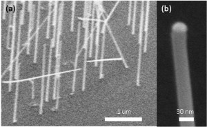
Figure 1: (a) An array of GaAs nanowires grown epitaxially by MOCVD, catalyzed by patterned Au/Cr metal features. (b) A 30-nm-diameter GaAs nanowire, with the metal catalyst clearly visible at the top of the nanowire.
Gold in particular has shown promise in producing oriented, size-selected nanowires [3]. This research significantly improves on the smallest lithographically-fabricated catalyst-particle size, while suppressing unwanted nanowires by controlling the migration of metal particles during the growth process and by preventing the self-catalysis of GaAs nanowires from the GaAs substrate.
Samples were prepared using GaAs substrates with 30 nm of evaporated silicon oxide deposited on top. The samples were patterned by electron-beam lithography, using a PMMA resist, and developed via a cold development process [4]. Pores were opened in the hard mask by HCF3/CF4 reactive-ion etching. After removal of the GaAs native oxide, metal catalyst nanoparticles were deposited into the pores by either electron-beam evaporation of Au, with a nominal thickness of 3 nm, or by galvanic displacement (GD) in a calibrated solution that also deposits 3 nm of Au. The GD solutions were prepared by dissolving hydrogen tetrachloroaurate(III) trihydrate (Alfa Aesar Co.) into deionized (DI) water. With either method, the sub-30-nm gold nanoparticles were fabricated.
References
- J. Goldberger, A.I. Hochbaum, R. Fan, and P. Yang, “Silicon vertically integrated nanowire field effect. Transistors,” Nano Lett., vol. 6, p. 973, 2006. [↩]
- X. Duan, Y. Huang, Y. Cui, J. Wang, and C. M. Lieber, “Logic gates and computation from assembled nanowire building blocks,” Nature, vol. 409, p. 66, 2001. [↩]
- P. Nguyen, H.T. Ng, and M. Meyyappan, “Growth of individual vertical germanium nanowires,” Adv. Mater., vol. 17, p. 1773, 2005. [↩]
- B. Cord, C. Dames, and K.K. Berggren, “Robust shadow-mask evaporation via lithographically controlled undercut” J. Vac. Sci. Technol. B, vol. 24, p. 3139, 2006. [↩]