Study of High-temperature Nanostructure Photonic Crystals

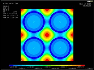
Figure 1: Simulated principal stress distribution in case of filled plug: the radial stress can go up to 1.5GPa at the interface.
More efficient solar thermal conversion systems can be developed by better controlling the energy conversion among photons, phonons, and electrons through micro-/nanostructured emitters and devices. One of the fundamental challenges, however, in solar-thermal energy conversion is the thermal stability of its materials and devices across a wide range of its operational temperatures. The micro-/nanostructured patterns of a thermal device would lose their structural integrity at high temperature, which would then disrupt the tightly machined tolerances required for spectral control of the thermal emitters, for example. We have investigated the thermal stability of nanostructured thermophotovoltaic emitters and have generated a design that may prevent the destruction of the surface nanostructure at temperatures above 1000° C.
Micro-/nano-patterned tungsten surfaces degrade substantially at temperatures over 1,000° C due to the excessive grain growth, recrystallization, and surface diffusion. The first task has been to explore the design idea and process options for plugging the empty holes of the tungsten PC with IR-transparent material. We expect that plugged holes with a high thermal expansion coefficient will generate compressive stress at high operating temperatures, which would suppress the excessive grain growth and recrystallization. In pursuit of this goal, the core plug material should have 1) high temperature resistance, 2) transparency to IR, 3) a reasonably bigger thermal expansion coefficient than that of tungsten, 4) large enough stiffness, and 5) a good diffusion barrier property compared to tungsten. Among possible candidates we considered (MgO and ZrO2), we chose ZrO2 for numerical simulation and concept-proving experiments. Figure 1a) shows the radial stress of a 2D tungsten PhC at 1000°C, where ZrO2 is filled in 700-nm diameter holes on W surface (the holes have a pitch of 850 nm). The radial stress at the W/ZrO2 boundary is 1.5 GPA.
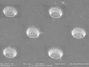
Fabrication of the simulated designs is under progress for actual experiments. As shown in Figure 2, a focused ion beam (FIB) has been used to pattern nano-holes on a tungsten substrate, which will be coated with TiN and subsequently filled with ZrO2. The samples will be fired at temperatures up to 1,000°C in order to compare the changes of the interface geometry with and without plugging.
