Spectral Selective Mid-infrared Detector on a Silicon Platform

Figure 1: Process flow to fabricate spectral selective mid-IR photodetectors on Si platform. Step 1: Bottom 1d-PC and PbTe photoactive layer deposition. Step 2: Top 1d-PC deposition and patterning. Step 3: Sn deposition and patterning.
Recently, people have shown increasing interest in spectral engineered mid-infrared (mid-IR) photodetectors due to their promising applications in chemical-biological sensing and hyperspectral imaging [1]. Spectral-selective detection has been demonstrated by two typical structures: integration of narrowband filters and broadband infrared detectors, and resonant-cavity-enhanced photodetectors. For the first type, incident IR light is filtered and then absorbed by photoactive layers. For the second type, a photoactive layer is sandwiched between two one-dimensional photonic crystals (1d-PC), forming a resonant cavity structure and providing highly wavelength-selective detection and high-quantum efficiency with a much thinner absorbing layer. However, previous structures rely on either polycrystalline PbSe films, which need a high-temperature-sensitization process, or expensive growth techniques such as molecular-beam epitaxy, which lack the capability of being monolithically integrated with Si read-out integrated circuit due to backside illumination and substrate limitation. A low-cost spectral engineered mid-IR photodetector technology that can be monolithically integrated on a silicon platform still remains to be explored.

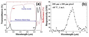
Figure 2: (a) Transmittance and reflectance spectra of the cavity structure. The photonic band gap is clearly seen in the range of 3.0 ~ 4.4 µm, and the cavity mode is shown in the reflectance spectrum at designed wavelength of 3.7 µm. (b) IR responsivity of a spectral selective photodetector at 1 mA bias current and at -60 oC, cooled by a thermoelectric cooler. The peak responsivity is 65.4 V/W and locates at 3.9 µm, which agrees quite well with the result in (a).
Here we demonstrate spectral-selective mid-IR photodetectors fabricated monolithically on a silicon platform, thereby significantly reducing the cost and improving device robustness. High-quality photoconductive polycrystalline PbTe film is thermally evaporated and acts as the IR absorber [2]. It is sandwiched between two highly reflective 1d-PC formed by evaporated As2S3 and sputtered Ge films. Figure 1 shows the fabrication process of the photodetector including two lift-off steps. Both transmittance and reflectance spectra are shown in Figure 2(a). In both spectra, the photonic band gap is clearly seen in the range of 3 ~ 4.4 µm. The cavity mode does not appear in the transmittance spectrum, but in the reflectance spectrum at the desired wavelength of 3.7 µm, indicating that this portion of light is absorbed by the PbTe layer. In Figure 2(b), the spectral selective detector shows a peak responsivity of 65.4 V/W at 3.9 µm, which agrees quite well with the result in Figure 2(a).
References
- A. Rogalski, J. Antoszewski, and L. Faraone, “Third-generation infrared photodetector arrays,” J. Appl. Phys., vol. 105, 091101, 2009. [↩]
- J. Wang, J. Hu, X. Sun, A. M. Agarwal, L. C. Kimerling, D. R. Lim, and R. A. Synowicki, “Structural, electrical, and optical properties of thermally evaporated nanocrystalline PbTe films,” J. Appl. Phys., vol. 104, 053707, 2008. [↩]