Simulated Secondary-electron trajectories in Helium-ion-beam Lithography
Scanning helium-ion-beam lithography (HIBL) can fabricate patterns with sub-10-nm half-pitch [1] [2]. The interaction volume of a beam with a sample is one measure of the spatial extent of energy deposition in that sample and thus of lithographic resolution. To evaluate limits on the interaction volume of a helium-ion beam and its generated secondary electrons (SEs) inside a resist layer, we have developed a Monte Carlo simulator using the software of Ziegler et al. [3], a parametric model for SE- generation by helium ions [4], and models for propagation of primary and “fast secondary” electrons [5] [6].
Figure 1 suggests that the contrast-reducing proximity effect, common in dense patterns written with ³10-keV electron-beam lithography (EBL), is absent for 30-keV HIBL. The interaction volume of the helium-ion beam is smaller than that of the electron beam, and no helium ions backscatter to the hydrogen silsesquioxane (HSQ) resist layer. HSQ was chosen for this simulation because of its status as a high-resolution EBL resist [7], because experiments by the authors – using HSQ – correspond with our electron model [8], and because HSQ has been used for sub-10-nm-half-pitch HIBL [1] [2].
Figure 2 suggests that, at least for resist thicknesses larger than a few nm, 30-keV HIBL can pattern smaller features than £30-keV EBL because the helium-ion beam does not fan out with depth as rapidly as the electron beams do (Figure 2(a)). However, it seems that SE-generation limits the interaction diameter of the helium-ion beam to ~ 2 nm because the helium-ion beam generates more SEs closer to the surface than do the electron beams (Figure 2(b)).
Our simulations suggest that HIBL may ultimately prove superior to EBL in the effort to simultaneously minimize (1) the proximity effect and (2) feature size, both of which limit resolvable half-pitch in resist-based lithography.
-
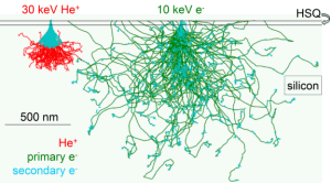
- Figure 1: Simulated trajectories of 100 30-keV helium ions (left) and 100 10-keV electrons (right), into 30-nm-thick HSQ resist on silicon. 10-keV electron landing energy was chosen because it is a typical low-end value for EBL. The trajectories of SEs generated by each particle beam are also simulated and plotted (light blue).
-
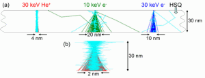
- Figure 2: (a) Simulated trajectories (1000 each) of 30-keV helium ions (left), 10-keV electrons (center), and 30-keV electrons (right), and also those of the SEs generated by each beam (light blue), in a 30-nm-thick “membrane” of HSQ resist. No trajectories are tracked below the HSQ, and thus no backscattered particles emerge from below the HSQ. Vertical and lateral scales are equal; (b) Magnified graphic of the 30-keV helium ions (red) and their generated SEs (light blue), where the lateral scale is stretched relative to the vertical scale to emphasize the SE tracks.
References
- D. Winston, B.M. Cord, B. Ming, D.C. Bell, W.F. DiNatale, L.A. Stern, A.E. Vladar, M.T. Postek, M.K. Mondol, J.K.W. Yang, and K.K. Berggren, “Scanning-helium-ion-beam lithography with hydrogen silsesquioxane resist,” J. Vac. Sci. Technol. B, vol. 27, pp. 2702-2706, 2009. [↩] [↩]
- V. Sidorkin, E. van Veldhoven, E. van der Drift, P. Alkemade, H. Salemink, and D. Maas, “Sub-10-nm nanolithography with a scanning helium beam,” J. Vac. Sci. Technol. B, vol. 27, pp. L18-L20, 2009. [↩] [↩]
- J.F. Ziegler, J.P. Biersack, and M.D. Ziegler, SRIM–The Stopping and Range of Ions in Matter. Chester, MD: SRIM Co.,2008. [↩]
- ref:4 [↩]
- R.A. Ghanbari, “Physics and fabrication of quasi-one-dimensional conductors,” Doctoral thesis, Massachusetts Institute of Technology, Cambridge, 1993. [↩]
- D.C. Joy, Monte Carlo Modeling for Electron Microscopy and Microanalysis. New York: Oxford University Press, 1995. [↩]
- J.K.W. Yang, B. Cord, H. Duan, K.K. Berggren, J. Klingfus, S. Nam, K. Kim, and M.J. Rooks, “Understanding of hydrogen silsesquioxane electron resist for sub-5-nm-half-pitch lithography,” J. Vac. Sci. Technol. B, vol. 27, pp. 2622-2627, 2009. [↩]
- L. Batistella, D. Winston, J. Ferrera, M. Mondol, and K.K. Berggren, in preparation. [↩]
Filed under: Materials, Nanotechnology |
Tags: donald winston, karl berggren
![]() Print This Page
Print This Page
![]() Download as PDF
Download as PDF