Silicon-nanopillar-based Nanocapacitor Structures Fabricated Using Metal-assisted Etching and Electrodeposition
Silicon nanowires (SiNWs) have attracted considerable attention due to potential applications arising from their quasi-one-dimensional structure. SiNWs, along with other nanowire and nanotube structures, are potential candidates for applications in nanoscale capacitors because of their large surface-to-volume ratio. However, although significant capacitance density increases have been demonstrated using these grown structures, issues such as high growth temperatures required for wires and tubes makes integration with current silicon technologies difficult. A room-temperature process such as metal-assisted etching (MAE) for the fabrication of high-aspect-ratio silicon nanostructures is therefore desired. In this approach metal catalysts are used to enhance local Si-etching at the metal-silicon interface in a mixture of hydrofluoric acid and an oxidant. The process can be used to fabricate high-aspect-ratio Si structures through patterned etching of silicon wafers. For example, we have used metal-assisted etching in conjunction with block copolymer lithography and post-etching critical-point drying to create silicon nanowire arrays with very high density and aspect ratio [1].
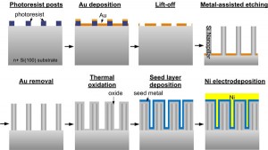
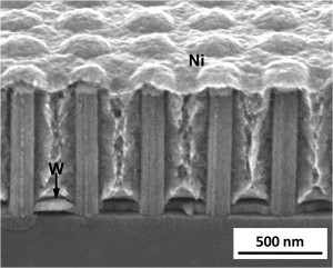
We have demonstrated the fabrication of silicon nanopillar-based nanocapacitor arrays using metal-assisted etching in conjunction with electrodeposition [2]. The high aspect ratio made possible by the catalyzed etching provides for an increased effective electrode area and hence a significant improvement in the capacitance density. The electroplated Ni electrode forms a conformal layer over the silicon nanopillars. The fabrication process is illustrated schematically in Figure 1. A square array of perforating holes in the metal catalyst thin film was created using interference lithography and metal lift-off processes. Figure 2 shows a scanning electron microscope (SEM) image of the capacitor structures. An increase in capacitance density as high as 8-fold compared to planar devices with the same oxide thickness was demonstrated using this method for a pillar array period of 200 nm and a pillar height of 1.5 μm. The capacitance scales as expected with the electrode area. In other studies, we have achieved much denser arrays of higher-aspect-ratio nanowires using block-copolymer lithography [2]. Capacitor structures made using these structures are expected to have a factor of ~100 capacitance increase compared to planar devices.
References
- S.W. Chang, J. Oh, S.T. Boles, and C.V. Thompson, “Fabrication of Silicon Nanopillar-based Nanocapacitor Arrays,” Appl. Phys. Letts. 96, 153108 (2010). [↩]
- S.W. Chang, V.P. Chuang, S.T. Boles, C.A. Ross, and C.V. Thompson, “Densely-packed arrays of ultrahigh-aspect-ratio silicon nanowire fabricated using block copolymer lithography and metal-assisted etching,” Adv. Funct. Mater., 19, 2495 (2009). [↩] [↩]

